Abdelaziz M. Aboraia, Shoroog Alraddadi, M. Saad, Yasser.A. M. Ismail, E. R. Shaaban
{"title":"Revealing the structural and optical constant of the UiO-66 coated with MoS2 QDs","authors":"Abdelaziz M. Aboraia, Shoroog Alraddadi, M. Saad, Yasser.A. M. Ismail, E. R. Shaaban","doi":"10.1007/s11082-024-07348-w","DOIUrl":null,"url":null,"abstract":"<div><p>We synthesized the pristine and MoS<sub>2</sub> QDs coated the UiO-66 nanostructures employing an eco-friendly drop casting method and studied the physical properties of nanostructures by experimental methods. The X-ray diffraction analysis confirmed that all samples exhibit a singular cubic phase with space group Fm3m. The presence of MoS<sub>2</sub> quantum dots coating led to an observed growth in crystalline size and an increase in structural defects. A rise in the optical energy gap (4.02–5.05 eV) and an improvement in transmittance were noted as the concentration of coated MoS<sub>2</sub> quantum dots increased. The film thickness of UiO-66@X%MOS<sub>2</sub> (X% = 0, 10, 15, 20, and 25) was around 140 ± 5 nm and the increase in the concentration of MoS<sub>2</sub>QDs was found to be inversely proportional to the decrease in refractive index. The absolute part values of the dielectric constant (ε<sub>1</sub>) are more significant than the imaginary part (ε<sub>2</sub>). Optical conductivity decreases with the higher content of embedded MoS<sub>2</sub> QDs (from 2.75 × 10<sup>10</sup> to 1.75 × 10<sup>10</sup>) at wavelengths 300–250 nm. Thus, MoS<sub>2</sub> QDs-coated UiO-66 nanostructures show suitable potential applications in: optoelectronics, efficient conversion of energy, and numerous other works implemented in the sphere of nanotechnology.</p></div>","PeriodicalId":720,"journal":{"name":"Optical and Quantum Electronics","volume":"56 9","pages":""},"PeriodicalIF":4.0000,"publicationDate":"2024-09-11","publicationTypes":"Journal Article","fieldsOfStudy":null,"isOpenAccess":false,"openAccessPdf":"","citationCount":"0","resultStr":null,"platform":"Semanticscholar","paperid":null,"PeriodicalName":"Optical and Quantum Electronics","FirstCategoryId":"5","ListUrlMain":"https://link.springer.com/article/10.1007/s11082-024-07348-w","RegionNum":3,"RegionCategory":"工程技术","ArticlePicture":[],"TitleCN":null,"AbstractTextCN":null,"PMCID":null,"EPubDate":"","PubModel":"","JCR":"Q2","JCRName":"ENGINEERING, ELECTRICAL & ELECTRONIC","Score":null,"Total":0}
引用次数: 0
Abstract
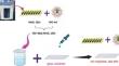
We synthesized the pristine and MoS2 QDs coated the UiO-66 nanostructures employing an eco-friendly drop casting method and studied the physical properties of nanostructures by experimental methods. The X-ray diffraction analysis confirmed that all samples exhibit a singular cubic phase with space group Fm3m. The presence of MoS2 quantum dots coating led to an observed growth in crystalline size and an increase in structural defects. A rise in the optical energy gap (4.02–5.05 eV) and an improvement in transmittance were noted as the concentration of coated MoS2 quantum dots increased. The film thickness of UiO-66@X%MOS2 (X% = 0, 10, 15, 20, and 25) was around 140 ± 5 nm and the increase in the concentration of MoS2QDs was found to be inversely proportional to the decrease in refractive index. The absolute part values of the dielectric constant (ε1) are more significant than the imaginary part (ε2). Optical conductivity decreases with the higher content of embedded MoS2 QDs (from 2.75 × 10¹⁰ to 1.75 × 10¹⁰) at wavelengths 300–250 nm. Thus, MoS2 QDs-coated UiO-66 nanostructures show suitable potential applications in: optoelectronics, efficient conversion of energy, and numerous other works implemented in the sphere of nanotechnology.
期刊介绍:
Optical and Quantum Electronics provides an international forum for the publication of original research papers, tutorial reviews and letters in such fields as optical physics, optical engineering and optoelectronics. Special issues are published on topics of current interest.
Optical and Quantum Electronics is published monthly. It is concerned with the technology and physics of optical systems, components and devices, i.e., with topics such as: optical fibres; semiconductor lasers and LEDs; light detection and imaging devices; nanophotonics; photonic integration and optoelectronic integrated circuits; silicon photonics; displays; optical communications from devices to systems; materials for photonics (e.g. semiconductors, glasses, graphene); the physics and simulation of optical devices and systems; nanotechnologies in photonics (including engineered nano-structures such as photonic crystals, sub-wavelength photonic structures, metamaterials, and plasmonics); advanced quantum and optoelectronic applications (e.g. quantum computing, memory and communications, quantum sensing and quantum dots); photonic sensors and bio-sensors; Terahertz phenomena; non-linear optics and ultrafast phenomena; green photonics.


 分享
分享
 求助内容:
求助内容: 应助结果提醒方式:
 扫码关注我们
