Subhajit Pal, Emanuele Palladino, Haozhen Yuan, Muireann Anna de h-Óra, Judith L. MacManus-Driscoll, Jorge Ontaneda, Vivek Dwij, Vasant G. Sathe, Joe Briscoe
{"title":"Determination of Imprint Effects in Ferroelectrics from the Quantified Phase and Amplitude Response","authors":"Subhajit Pal, Emanuele Palladino, Haozhen Yuan, Muireann Anna de h-Óra, Judith L. MacManus-Driscoll, Jorge Ontaneda, Vivek Dwij, Vasant G. Sathe, Joe Briscoe","doi":"10.1021/acsaelm.4c00875","DOIUrl":null,"url":null,"abstract":"Piezoresponse force microscopy (PFM) is a robust characterization technique to explore ferroelectric properties at the nanoscale. However, the PFM signal can lead to misinterpretation of results due to the dominant electrostatic interaction between the tip and the sample. In this work, a detailed calibration process is presented and a procedure to identify the parasitic phase offset is demonstrated. To obtain artifact-free phase–amplitude loops, a methodology is developed by combining the outcomes from switching spectroscopy-PFM (SS-PFM) and Kelvin probe force microscopy (KPFM). It is demonstrated that the phase and amplitude loops obtained from SS-PFM at a specific read voltage, ascertained from the surface potential by KPFM, can convey accurate electromechanical information. These methodologies are applied to quantify the imprint voltage in BaTiO<sub>3</sub> and BiFeO<sub>3</sub>, along with vertically aligned BaTiO<sub>3</sub>:Sm<sub>2</sub>O<sub>3</sub> and BaTiO<sub>3</sub>:MgO nanocomposites. The variation of the imprint voltage measured under different tip voltages demonstrates the importance of selecting the correct read voltage in determining the local imprint voltage. Additionally, 2D imprint voltage maps in each domain of a BaTiO<sub>3</sub> single crystal are obtained using the datacube-PFM technique, which allows pixel-by-pixel determination of artifact-free spatial variation of PFM phase–amplitude response.","PeriodicalId":3,"journal":{"name":"ACS Applied Electronic Materials","volume":"15 1","pages":""},"PeriodicalIF":4.7000,"publicationDate":"2024-09-15","publicationTypes":"Journal Article","fieldsOfStudy":null,"isOpenAccess":false,"openAccessPdf":"","citationCount":"0","resultStr":null,"platform":"Semanticscholar","paperid":null,"PeriodicalName":"ACS Applied Electronic Materials","FirstCategoryId":"88","ListUrlMain":"https://doi.org/10.1021/acsaelm.4c00875","RegionNum":3,"RegionCategory":"材料科学","ArticlePicture":[],"TitleCN":null,"AbstractTextCN":null,"PMCID":null,"EPubDate":"","PubModel":"","JCR":"Q1","JCRName":"ENGINEERING, ELECTRICAL & ELECTRONIC","Score":null,"Total":0}
引用次数: 0
Abstract
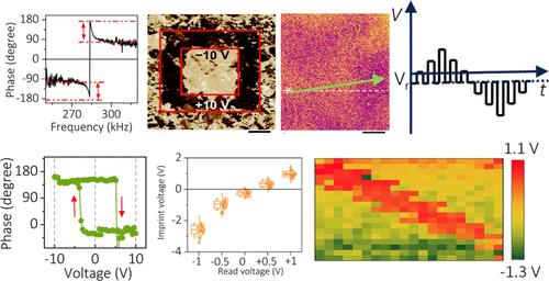
Piezoresponse force microscopy (PFM) is a robust characterization technique to explore ferroelectric properties at the nanoscale. However, the PFM signal can lead to misinterpretation of results due to the dominant electrostatic interaction between the tip and the sample. In this work, a detailed calibration process is presented and a procedure to identify the parasitic phase offset is demonstrated. To obtain artifact-free phase–amplitude loops, a methodology is developed by combining the outcomes from switching spectroscopy-PFM (SS-PFM) and Kelvin probe force microscopy (KPFM). It is demonstrated that the phase and amplitude loops obtained from SS-PFM at a specific read voltage, ascertained from the surface potential by KPFM, can convey accurate electromechanical information. These methodologies are applied to quantify the imprint voltage in BaTiO3 and BiFeO3, along with vertically aligned BaTiO3:Sm2O3 and BaTiO3:MgO nanocomposites. The variation of the imprint voltage measured under different tip voltages demonstrates the importance of selecting the correct read voltage in determining the local imprint voltage. Additionally, 2D imprint voltage maps in each domain of a BaTiO3 single crystal are obtained using the datacube-PFM technique, which allows pixel-by-pixel determination of artifact-free spatial variation of PFM phase–amplitude response.
期刊介绍:
ACS Applied Electronic Materials is an interdisciplinary journal publishing original research covering all aspects of electronic materials. The journal is devoted to reports of new and original experimental and theoretical research of an applied nature that integrate knowledge in the areas of materials science, engineering, optics, physics, and chemistry into important applications of electronic materials. Sample research topics that span the journal's scope are inorganic, organic, ionic and polymeric materials with properties that include conducting, semiconducting, superconducting, insulating, dielectric, magnetic, optoelectronic, piezoelectric, ferroelectric and thermoelectric.
Indexed/Abstracted:
Web of Science SCIE
Scopus
CAS
INSPEC
Portico


 分享
分享
 求助内容:
求助内容: 应助结果提醒方式:
 扫码关注我们
