{"title":"High responsivity zero-biased Mid-IR graphene photodetector based on chalcogenide glass waveguide","authors":"Hadi Hashemnezhad , Mina Noori","doi":"10.1016/j.optlastec.2024.111852","DOIUrl":null,"url":null,"abstract":"<div><div>Graphene’s unique properties have made it a promising material for high-performance photodetectors due to its interesting features including broadband absorption, fast speed, and strong photothermoelectric effect. Here, an optimized waveguide photodetector incorporating double graphene layers with two cores is presented to boost the responsivity (∼twice), at Mid-IR range. The proposed structure operates in the zero-bias regime to eliminate the dark current issue associated with the zero bandgap nature of graphene and leads to lower noise equivalent power. The presented photodetector operating based on split gates to electrostatically induce the p-n junction in graphene channels, operates based on the photothermoelectric effect and provides responsivity, NEP, and 3 dB bandwidth of 6.3 V/W, 0.34 nW/Hz<sup>1/2</sup>, and 1.54 GHz, respectively for the detection at λ = 5.2 μm. The feasibility of the proposed structure is proved according to recent experimentally demonstrated photodetectors. Hence, the obtained results are reliable, in practice. The study has been accomplished by numerical simulation of mode profiles and solving the heat equation to extract the characteristics of the proposed photodetector. The zero-power consumption and tunability of the proposed structure make it a promising candidate for sensing, industrial, defense, and environmental monitoring applications with high accuracy.</div></div>","PeriodicalId":19511,"journal":{"name":"Optics and Laser Technology","volume":"181 ","pages":"Article 111852"},"PeriodicalIF":5.0000,"publicationDate":"2025-02-01","publicationTypes":"Journal Article","fieldsOfStudy":null,"isOpenAccess":false,"openAccessPdf":"","citationCount":"0","resultStr":null,"platform":"Semanticscholar","paperid":null,"PeriodicalName":"Optics and Laser Technology","FirstCategoryId":"101","ListUrlMain":"https://www.sciencedirect.com/science/article/pii/S0030399224013100","RegionNum":2,"RegionCategory":"物理与天体物理","ArticlePicture":[],"TitleCN":null,"AbstractTextCN":null,"PMCID":null,"EPubDate":"2024/9/26 0:00:00","PubModel":"Epub","JCR":"Q1","JCRName":"OPTICS","Score":null,"Total":0}
引用次数: 0
Abstract
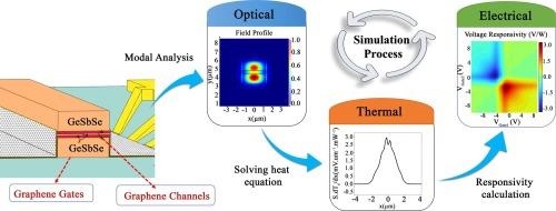
Graphene’s unique properties have made it a promising material for high-performance photodetectors due to its interesting features including broadband absorption, fast speed, and strong photothermoelectric effect. Here, an optimized waveguide photodetector incorporating double graphene layers with two cores is presented to boost the responsivity (∼twice), at Mid-IR range. The proposed structure operates in the zero-bias regime to eliminate the dark current issue associated with the zero bandgap nature of graphene and leads to lower noise equivalent power. The presented photodetector operating based on split gates to electrostatically induce the p-n junction in graphene channels, operates based on the photothermoelectric effect and provides responsivity, NEP, and 3 dB bandwidth of 6.3 V/W, 0.34 nW/Hz1/2, and 1.54 GHz, respectively for the detection at λ = 5.2 μm. The feasibility of the proposed structure is proved according to recent experimentally demonstrated photodetectors. Hence, the obtained results are reliable, in practice. The study has been accomplished by numerical simulation of mode profiles and solving the heat equation to extract the characteristics of the proposed photodetector. The zero-power consumption and tunability of the proposed structure make it a promising candidate for sensing, industrial, defense, and environmental monitoring applications with high accuracy.
期刊介绍:
Optics & Laser Technology aims to provide a vehicle for the publication of a broad range of high quality research and review papers in those fields of scientific and engineering research appertaining to the development and application of the technology of optics and lasers. Papers describing original work in these areas are submitted to rigorous refereeing prior to acceptance for publication.
The scope of Optics & Laser Technology encompasses, but is not restricted to, the following areas:
•development in all types of lasers
•developments in optoelectronic devices and photonics
•developments in new photonics and optical concepts
•developments in conventional optics, optical instruments and components
•techniques of optical metrology, including interferometry and optical fibre sensors
•LIDAR and other non-contact optical measurement techniques, including optical methods in heat and fluid flow
•applications of lasers to materials processing, optical NDT display (including holography) and optical communication
•research and development in the field of laser safety including studies of hazards resulting from the applications of lasers (laser safety, hazards of laser fume)
•developments in optical computing and optical information processing
•developments in new optical materials
•developments in new optical characterization methods and techniques
•developments in quantum optics
•developments in light assisted micro and nanofabrication methods and techniques
•developments in nanophotonics and biophotonics
•developments in imaging processing and systems


 分享
分享
 求助内容:
求助内容: 应助结果提醒方式:
 扫码关注我们
