Shalini Kumari , Neha Dhull , Weichang Lin , Zonghuan Lu , Joan Redwing , Toh-Ming Lu , Gwo-Ching Wang
{"title":"In-plane and out-of-plane domain orientation dispersions in 1 to 3 monolayers epitaxial WS2 and MoS2 films on GaN(0001) film/sapphire(0001)","authors":"Shalini Kumari , Neha Dhull , Weichang Lin , Zonghuan Lu , Joan Redwing , Toh-Ming Lu , Gwo-Ching Wang","doi":"10.1016/j.physe.2024.116117","DOIUrl":null,"url":null,"abstract":"<div><div>Transition-metal dichalcogenides and their heterostructures have attractive potential applications in electronics and optoelectronics. Wafer scale 1 to 3 monolayers WS<sub>2</sub> and MoS<sub>2</sub> ultrathin films on GaN/sapphire substrates were grown by metal organic chemical vapor deposition. Azimuthal reflection high-energy electron diffraction (ARHEED) was used to characterize the long-range order of these TMDC ultrathin films. The RHEED patterns of WS<sub>2</sub> and MoS<sub>2</sub> show stripes and arcs but the MoS<sub>2</sub> on GaN shows sharp spots in addition to stripes and arcs. The 2D map constructed from ARHEED patterns shows that WS<sub>2</sub> is epitaxial and has an in-plane domain orientation dispersion. For the MoS<sub>2</sub> on GaN/sapphire substrate, the 2D map shows concentric continuous rings for each diffraction order of MoS<sub>2</sub> and GaN indicating that the in-plane MoS<sub>2</sub> domain orientation and GaN nanocrystals are random. The out-of-plane orientation dispersion of MoS<sub>2</sub> on the GaN substrate is larger than that of WS<sub>2</sub> on the GaN substrate. The observations of stripes, arcs, and spots from RHEED patterns and the 2D maps reveal the deviation of ultrathin epitaxial films from its perfect epitaxy, especially the TMDC domain orientation dispersion over a large area. These rich findings from 2D maps broaden the application of ARHEED in more than one monolayer thick 2D materials.</div></div>","PeriodicalId":20181,"journal":{"name":"Physica E-low-dimensional Systems & Nanostructures","volume":"165 ","pages":"Article 116117"},"PeriodicalIF":2.9000,"publicationDate":"2024-10-01","publicationTypes":"Journal Article","fieldsOfStudy":null,"isOpenAccess":false,"openAccessPdf":"","citationCount":"0","resultStr":null,"platform":"Semanticscholar","paperid":null,"PeriodicalName":"Physica E-low-dimensional Systems & Nanostructures","FirstCategoryId":"101","ListUrlMain":"https://www.sciencedirect.com/science/article/pii/S1386947724002212","RegionNum":3,"RegionCategory":"物理与天体物理","ArticlePicture":[],"TitleCN":null,"AbstractTextCN":null,"PMCID":null,"EPubDate":"","PubModel":"","JCR":"Q3","JCRName":"NANOSCIENCE & NANOTECHNOLOGY","Score":null,"Total":0}
引用次数: 0
Abstract
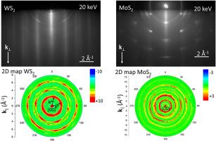
Transition-metal dichalcogenides and their heterostructures have attractive potential applications in electronics and optoelectronics. Wafer scale 1 to 3 monolayers WS2 and MoS2 ultrathin films on GaN/sapphire substrates were grown by metal organic chemical vapor deposition. Azimuthal reflection high-energy electron diffraction (ARHEED) was used to characterize the long-range order of these TMDC ultrathin films. The RHEED patterns of WS2 and MoS2 show stripes and arcs but the MoS2 on GaN shows sharp spots in addition to stripes and arcs. The 2D map constructed from ARHEED patterns shows that WS2 is epitaxial and has an in-plane domain orientation dispersion. For the MoS2 on GaN/sapphire substrate, the 2D map shows concentric continuous rings for each diffraction order of MoS2 and GaN indicating that the in-plane MoS2 domain orientation and GaN nanocrystals are random. The out-of-plane orientation dispersion of MoS2 on the GaN substrate is larger than that of WS2 on the GaN substrate. The observations of stripes, arcs, and spots from RHEED patterns and the 2D maps reveal the deviation of ultrathin epitaxial films from its perfect epitaxy, especially the TMDC domain orientation dispersion over a large area. These rich findings from 2D maps broaden the application of ARHEED in more than one monolayer thick 2D materials.
期刊介绍:
Physica E: Low-dimensional systems and nanostructures contains papers and invited review articles on the fundamental and applied aspects of physics in low-dimensional electron systems, in semiconductor heterostructures, oxide interfaces, quantum wells and superlattices, quantum wires and dots, novel quantum states of matter such as topological insulators, and Weyl semimetals.
Both theoretical and experimental contributions are invited. Topics suitable for publication in this journal include spin related phenomena, optical and transport properties, many-body effects, integer and fractional quantum Hall effects, quantum spin Hall effect, single electron effects and devices, Majorana fermions, and other novel phenomena.
Keywords:
• topological insulators/superconductors, majorana fermions, Wyel semimetals;
• quantum and neuromorphic computing/quantum information physics and devices based on low dimensional systems;
• layered superconductivity, low dimensional systems with superconducting proximity effect;
• 2D materials such as transition metal dichalcogenides;
• oxide heterostructures including ZnO, SrTiO3 etc;
• carbon nanostructures (graphene, carbon nanotubes, diamond NV center, etc.)
• quantum wells and superlattices;
• quantum Hall effect, quantum spin Hall effect, quantum anomalous Hall effect;
• optical- and phonons-related phenomena;
• magnetic-semiconductor structures;
• charge/spin-, magnon-, skyrmion-, Cooper pair- and majorana fermion- transport and tunneling;
• ultra-fast nonlinear optical phenomena;
• novel devices and applications (such as high performance sensor, solar cell, etc);
• novel growth and fabrication techniques for nanostructures


 分享
分享
 求助内容:
求助内容: 应助结果提醒方式:
 扫码关注我们
