Anna C. Kundmann, Kathleen Becker and Frank E. Osterloh
{"title":"Surface photovoltage predicts open circuit voltage in GaP/PEDOT:PSS and GaP/CuSCN heterojunction solar cells†","authors":"Anna C. Kundmann, Kathleen Becker and Frank E. Osterloh","doi":"10.1039/D4LF00225C","DOIUrl":null,"url":null,"abstract":"<p >The cost-effective fabrication of inorganic photovoltaic (PV) devices is important for their implementation on a global scale. Solution processing techniques, such as spray coating, spin coating, and electrodeposition, can drive down costs; however, a better understanding of the charge transfer characteristics of the resulting semiconductor heterojunctions is needed to minimize photovoltage losses at interfaces. In this work, we generate solution-processed heterojunctions by spin coating PEDOT:PSS and electrodepositing CuSCN as hole transport layers (HTLs) onto GaP wafers. After adding silver paint as a front contact, we obtain devices with short circuit current densities of 0.40 mA cm<small><sup>−2</sup></small> and 0.18 mA cm<small><sup>−2</sup></small>, open circuit voltages of 0.47 V and 0.43 V, and power conversion efficiencies of 0.045% and 0.031% for PEDOT:PSS and CuSCN HTLs, respectively. Surface photovoltage spectroscopy (SPS) is used to study photochemical charge separation at the illuminated GaP interfaces. We find that the surface photovoltage signal is a good predictor of the photovoltage of the devices, as confirmed by comparison with open circuit potential data. SPS also reveals improved hole collection by the HTLs and a detrimental Schottky junction at the In/GaP back contact, further evidenced by S-shaped current–voltage profiles in electric measurements. Reducing the Schottky barrier height will be essential to improve device performance.</p>","PeriodicalId":101138,"journal":{"name":"RSC Applied Interfaces","volume":" 6","pages":" 1426-1435"},"PeriodicalIF":0.0000,"publicationDate":"2024-09-20","publicationTypes":"Journal Article","fieldsOfStudy":null,"isOpenAccess":false,"openAccessPdf":"https://pubs.rsc.org/en/content/articlepdf/2024/lf/d4lf00225c?page=search","citationCount":"0","resultStr":null,"platform":"Semanticscholar","paperid":null,"PeriodicalName":"RSC Applied Interfaces","FirstCategoryId":"1085","ListUrlMain":"https://pubs.rsc.org/en/content/articlelanding/2024/lf/d4lf00225c","RegionNum":0,"RegionCategory":null,"ArticlePicture":[],"TitleCN":null,"AbstractTextCN":null,"PMCID":null,"EPubDate":"","PubModel":"","JCR":"","JCRName":"","Score":null,"Total":0}
引用次数: 0
Abstract
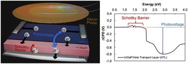
The cost-effective fabrication of inorganic photovoltaic (PV) devices is important for their implementation on a global scale. Solution processing techniques, such as spray coating, spin coating, and electrodeposition, can drive down costs; however, a better understanding of the charge transfer characteristics of the resulting semiconductor heterojunctions is needed to minimize photovoltage losses at interfaces. In this work, we generate solution-processed heterojunctions by spin coating PEDOT:PSS and electrodepositing CuSCN as hole transport layers (HTLs) onto GaP wafers. After adding silver paint as a front contact, we obtain devices with short circuit current densities of 0.40 mA cm−2 and 0.18 mA cm−2, open circuit voltages of 0.47 V and 0.43 V, and power conversion efficiencies of 0.045% and 0.031% for PEDOT:PSS and CuSCN HTLs, respectively. Surface photovoltage spectroscopy (SPS) is used to study photochemical charge separation at the illuminated GaP interfaces. We find that the surface photovoltage signal is a good predictor of the photovoltage of the devices, as confirmed by comparison with open circuit potential data. SPS also reveals improved hole collection by the HTLs and a detrimental Schottky junction at the In/GaP back contact, further evidenced by S-shaped current–voltage profiles in electric measurements. Reducing the Schottky barrier height will be essential to improve device performance.


 分享
分享

 求助内容:
求助内容: 应助结果提醒方式:
 扫码关注我们
