Vaishali Vardhan, Subhajit Biswas, Sayantan Ghosh, Leonidas Tsetseris, Tandra Ghoshal, Stig Hellebust, Yordan M. Georgiev, Justin D. Holmes
{"title":"Pseudo Molecular Doping and Ambipolarity Tuning in Si Junctionless Nanowire Transistors Using Gaseous Nitrogen Dioxide","authors":"Vaishali Vardhan, Subhajit Biswas, Sayantan Ghosh, Leonidas Tsetseris, Tandra Ghoshal, Stig Hellebust, Yordan M. Georgiev, Justin D. Holmes","doi":"10.1002/aelm.202400338","DOIUrl":null,"url":null,"abstract":"<p>Ambipolar transistors facilitate concurrent transport of both positive (holes) and negative (electrons) charge carriers in the semiconducting channel. Effective manipulation of conduction symmetry and electrical characteristics in ambipolar silicon junctionless nanowire transistors (Si-JNTs) is demonstrated using gaseous nitrogen dioxide (NO<sub>2</sub>). This involves a dual reaction in both <i>p</i>- and <i>n</i>-type conduction, resulting in a significant decrease in the current in <i>n</i>-conduction mode and an increase in the <i>p</i>-conduction mode upon NO<sub>2</sub> exposure. Various Si-JNT parameters, including “on”-current (<i>I<sub>on</sub></i>), threshold voltage (<i>V<sub>th</sub></i>), and mobility (<i>µ</i>) exhibit dynamic changes in both the <i>p</i>- and <i>n</i>-conduction modes of the ambipolar transistor upon interaction with NO<sub>2</sub> (concentration between 2.5 – 50 ppm). Additionally, NO<sub>2</sub> exposure to Si-JNTs with different surface morphologies, that is, unpassivated Si-JNTs with a native oxide or with a thermally grown oxide (10 nm), show distinct influences on <i>I<sub>on</sub></i>, <i>V<sub>th</sub></i>, and <i>µ</i>, highlighting the effect of surface oxide on NO<sub>2</sub>-mediated charge transfer. Interaction with NO<sub>2</sub> alters the carrier concentration in the JNT channel, with NO<sub>2</sub> acting as an electron acceptor and inducing holes, as supported by Density Functional Theory (DFT) calculations, providing a pathway for charge transfer and “pseudo” molecular doping in ambipolar Si-JNTs.</p>","PeriodicalId":110,"journal":{"name":"Advanced Electronic Materials","volume":"11 2","pages":""},"PeriodicalIF":5.3000,"publicationDate":"2024-11-19","publicationTypes":"Journal Article","fieldsOfStudy":null,"isOpenAccess":false,"openAccessPdf":"https://onlinelibrary.wiley.com/doi/epdf/10.1002/aelm.202400338","citationCount":"0","resultStr":null,"platform":"Semanticscholar","paperid":null,"PeriodicalName":"Advanced Electronic Materials","FirstCategoryId":"88","ListUrlMain":"https://advanced.onlinelibrary.wiley.com/doi/10.1002/aelm.202400338","RegionNum":2,"RegionCategory":"材料科学","ArticlePicture":[],"TitleCN":null,"AbstractTextCN":null,"PMCID":null,"EPubDate":"","PubModel":"","JCR":"Q2","JCRName":"MATERIALS SCIENCE, MULTIDISCIPLINARY","Score":null,"Total":0}
引用次数: 0
Abstract
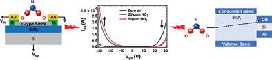
Ambipolar transistors facilitate concurrent transport of both positive (holes) and negative (electrons) charge carriers in the semiconducting channel. Effective manipulation of conduction symmetry and electrical characteristics in ambipolar silicon junctionless nanowire transistors (Si-JNTs) is demonstrated using gaseous nitrogen dioxide (NO2). This involves a dual reaction in both p- and n-type conduction, resulting in a significant decrease in the current in n-conduction mode and an increase in the p-conduction mode upon NO2 exposure. Various Si-JNT parameters, including “on”-current (Ion), threshold voltage (Vth), and mobility (µ) exhibit dynamic changes in both the p- and n-conduction modes of the ambipolar transistor upon interaction with NO2 (concentration between 2.5 – 50 ppm). Additionally, NO2 exposure to Si-JNTs with different surface morphologies, that is, unpassivated Si-JNTs with a native oxide or with a thermally grown oxide (10 nm), show distinct influences on Ion, Vth, and µ, highlighting the effect of surface oxide on NO2-mediated charge transfer. Interaction with NO2 alters the carrier concentration in the JNT channel, with NO2 acting as an electron acceptor and inducing holes, as supported by Density Functional Theory (DFT) calculations, providing a pathway for charge transfer and “pseudo” molecular doping in ambipolar Si-JNTs.
期刊介绍:
Advanced Electronic Materials is an interdisciplinary forum for peer-reviewed, high-quality, high-impact research in the fields of materials science, physics, and engineering of electronic and magnetic materials. It includes research on physics and physical properties of electronic and magnetic materials, spintronics, electronics, device physics and engineering, micro- and nano-electromechanical systems, and organic electronics, in addition to fundamental research.


 分享
分享
 求助内容:
求助内容: 应助结果提醒方式:
 扫码关注我们
