{"title":"Interface engineering for minimizing trapped charge density in β-Ga₂O₃ Schottky barrier diodes for high-performance power devices","authors":"Shivani , Atul G. Chakkar , Pradeep Kumar , Mukesh Kumar","doi":"10.1016/j.mtphys.2024.101605","DOIUrl":null,"url":null,"abstract":"<div><div>Gallium oxide (Ga<sub>2</sub>O<sub>3</sub>), with its ultra-wide bandgap and high breakdown voltage, has emerged as a leading candidate for next-generation power devices. The performance and the Baliga figure-of-merit for power devices critically depend on breakdown voltage sustained by Schottky contact of metal with ultra-wide gap materials. However, high-quality Schottky contacts with Ga<sub>2</sub>O<sub>3</sub> presents a significant challenge due to the presence of surface defects and formation of metal induced mid-gap defects states in Ga<sub>2</sub>O<sub>3</sub>. In this study, we investigate the electrical properties and defects at the interface between Ni metal and <em>β</em>-Ga₂O₃ thin films. Additionally, a 20 nm MgO thin films with various oxygen contents were deposited on β-Ga<sub>2</sub>O<sub>3</sub> using radio-frequency magnetron sputtering and Ni/MgO/<em>β</em>-Ga<sub>2</sub>O<sub>3</sub> metal-insulator-semiconductor Schottky diodes were fabricated. The frequency dependent C-V characteristic and surface-sensitive XPS depth profile is employed to study the interface of Ni/Ga<sub>2</sub>O<sub>3</sub> and Ni/MgO/Ga<sub>2</sub>O<sub>3</sub> Schottky barrier diodes. Our results show that the Ni/MgO/Ga₂O₃ Schottky barrier diode with 66 % O₂ in the MgO thin film during synthesis attains a barrier height of 0.87 eV. Subsequent post-metallization annealing at 300 °C in an Ar ambient for 30 min enhances the barrier height up to 1.1 eV. Also, a reduced on-resistance of 11.65 mΩ cm<sup>2</sup> and a lower on-voltage of 0.3V was obtained after annealing in Ar. The frequency dependent <em>C-V</em> characteristic results show no dispersion in capacitance for the annealed sample which signify the passivation of interface defects density (Δ<sub>ιτ</sub>) and oxide charges density (N<sub>f</sub>) in the dielectric layer (MgO). The minimum value of D<sub>it</sub> and N<sub>f</sub> achieved for the sample having highest barrier height (1.1eV) are 5.41 × 10<sup>11</sup>/eV/cm<sup>2</sup> and 2.91 × 10<sup>10</sup>/cm<sup>3</sup>, respectively. This study establishes a vigorous foundation for the expanded utilization of Ga<sub>2</sub>O<sub>3</sub> in power electronics devices, emphasizing the vital role of interface engineering.</div></div>","PeriodicalId":18253,"journal":{"name":"Materials Today Physics","volume":"50 ","pages":"Article 101605"},"PeriodicalIF":9.7000,"publicationDate":"2025-01-01","publicationTypes":"Journal Article","fieldsOfStudy":null,"isOpenAccess":false,"openAccessPdf":"","citationCount":"0","resultStr":null,"platform":"Semanticscholar","paperid":null,"PeriodicalName":"Materials Today Physics","FirstCategoryId":"88","ListUrlMain":"https://www.sciencedirect.com/science/article/pii/S2542529324002815","RegionNum":2,"RegionCategory":"材料科学","ArticlePicture":[],"TitleCN":null,"AbstractTextCN":null,"PMCID":null,"EPubDate":"2024/11/28 0:00:00","PubModel":"Epub","JCR":"Q1","JCRName":"MATERIALS SCIENCE, MULTIDISCIPLINARY","Score":null,"Total":0}
引用次数: 0
Abstract
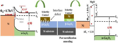
Gallium oxide (Ga2O3), with its ultra-wide bandgap and high breakdown voltage, has emerged as a leading candidate for next-generation power devices. The performance and the Baliga figure-of-merit for power devices critically depend on breakdown voltage sustained by Schottky contact of metal with ultra-wide gap materials. However, high-quality Schottky contacts with Ga2O3 presents a significant challenge due to the presence of surface defects and formation of metal induced mid-gap defects states in Ga2O3. In this study, we investigate the electrical properties and defects at the interface between Ni metal and β-Ga₂O₃ thin films. Additionally, a 20 nm MgO thin films with various oxygen contents were deposited on β-Ga2O3 using radio-frequency magnetron sputtering and Ni/MgO/β-Ga2O3 metal-insulator-semiconductor Schottky diodes were fabricated. The frequency dependent C-V characteristic and surface-sensitive XPS depth profile is employed to study the interface of Ni/Ga2O3 and Ni/MgO/Ga2O3 Schottky barrier diodes. Our results show that the Ni/MgO/Ga₂O₃ Schottky barrier diode with 66 % O₂ in the MgO thin film during synthesis attains a barrier height of 0.87 eV. Subsequent post-metallization annealing at 300 °C in an Ar ambient for 30 min enhances the barrier height up to 1.1 eV. Also, a reduced on-resistance of 11.65 mΩ cm2 and a lower on-voltage of 0.3V was obtained after annealing in Ar. The frequency dependent C-V characteristic results show no dispersion in capacitance for the annealed sample which signify the passivation of interface defects density (Διτ) and oxide charges density (Nf) in the dielectric layer (MgO). The minimum value of Dit and Nf achieved for the sample having highest barrier height (1.1eV) are 5.41 × 10¹¹/eV/cm2 and 2.91 × 10¹⁰/cm3, respectively. This study establishes a vigorous foundation for the expanded utilization of Ga2O3 in power electronics devices, emphasizing the vital role of interface engineering.
期刊介绍:
Materials Today Physics is a multi-disciplinary journal focused on the physics of materials, encompassing both the physical properties and materials synthesis. Operating at the interface of physics and materials science, this journal covers one of the largest and most dynamic fields within physical science. The forefront research in materials physics is driving advancements in new materials, uncovering new physics, and fostering novel applications at an unprecedented pace.


 分享
分享
 求助内容:
求助内容: 应助结果提醒方式:
 扫码关注我们
