{"title":"Topographic Scanning Electronic Microscopy Reveals the 3D Surface Structure of Materials","authors":"Wen Sun, Yichen Xu, Ying Zhou, Zhihan Zeng, Lei Wang, Jianyong Ouyang","doi":"10.1002/adfm.202420372","DOIUrl":null,"url":null,"abstract":"<p>Scanning electron microscopy (SEM) is a very popular technology to analyze the surface morphology of various materials in both academia and industry. Its principle is the detection of secondary electron emission and electron scattering interactions between the electron beam and the sample surface. It requires the deposition of a thin metal film like Au on non-conductive samples to prevent charge accumulation. However, due to the discontinuity of the Au film along the vertical direction of a sample, the SEM images cannot provide information along the vertical direction. Additionally, the gold films have grains of 10–12 nm in diameter, which can limit the resolution of the SEM images. Here, topographic SEM is reported by coating poly(3,4-ethylenedioxythiophene):poly(styrenesulfonate) (PEDOT:PSS, an intrinsically conductive polymer) onto samples instead of metal deposition. High-quality features along both the horizontal and vertical directions can be observed on the SEM images because PEDOT:PSS can form a continuous film along both directions. Furthermore, due to the featureless morphology of the PEDOT:PSS films, the resolution of SEM images is significantly higher than that with gold deposition. The application of topographical SEM in the characterization of various materials, including patterned semiconductors, nanostructured materials, energy materials, biomaterials, etc is demonstrated.</p>","PeriodicalId":112,"journal":{"name":"Advanced Functional Materials","volume":"35 17","pages":""},"PeriodicalIF":19.0000,"publicationDate":"2024-12-19","publicationTypes":"Journal Article","fieldsOfStudy":null,"isOpenAccess":false,"openAccessPdf":"","citationCount":"0","resultStr":null,"platform":"Semanticscholar","paperid":null,"PeriodicalName":"Advanced Functional Materials","FirstCategoryId":"88","ListUrlMain":"https://advanced.onlinelibrary.wiley.com/doi/10.1002/adfm.202420372","RegionNum":1,"RegionCategory":"材料科学","ArticlePicture":[],"TitleCN":null,"AbstractTextCN":null,"PMCID":null,"EPubDate":"","PubModel":"","JCR":"Q1","JCRName":"CHEMISTRY, MULTIDISCIPLINARY","Score":null,"Total":0}
引用次数: 0
Abstract
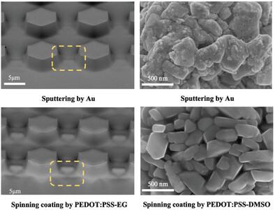
Scanning electron microscopy (SEM) is a very popular technology to analyze the surface morphology of various materials in both academia and industry. Its principle is the detection of secondary electron emission and electron scattering interactions between the electron beam and the sample surface. It requires the deposition of a thin metal film like Au on non-conductive samples to prevent charge accumulation. However, due to the discontinuity of the Au film along the vertical direction of a sample, the SEM images cannot provide information along the vertical direction. Additionally, the gold films have grains of 10–12 nm in diameter, which can limit the resolution of the SEM images. Here, topographic SEM is reported by coating poly(3,4-ethylenedioxythiophene):poly(styrenesulfonate) (PEDOT:PSS, an intrinsically conductive polymer) onto samples instead of metal deposition. High-quality features along both the horizontal and vertical directions can be observed on the SEM images because PEDOT:PSS can form a continuous film along both directions. Furthermore, due to the featureless morphology of the PEDOT:PSS films, the resolution of SEM images is significantly higher than that with gold deposition. The application of topographical SEM in the characterization of various materials, including patterned semiconductors, nanostructured materials, energy materials, biomaterials, etc is demonstrated.
期刊介绍:
Firmly established as a top-tier materials science journal, Advanced Functional Materials reports breakthrough research in all aspects of materials science, including nanotechnology, chemistry, physics, and biology every week.
Advanced Functional Materials is known for its rapid and fair peer review, quality content, and high impact, making it the first choice of the international materials science community.


 分享
分享
 求助内容:
求助内容: 应助结果提醒方式:
 扫码关注我们
