Gihyeon Kwon, Hyeon-Sik Kim, Kwangsik Jeong, Sewoong Oh, Dajung Kim, Woochan Koh, Hyunjun Park, Seongil Im, Mann-Ho Cho
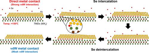
{"title":"Reconfiguring van der Waals Metal–Semiconductor Contacts via Selenium Intercalation/Deintercalation Post-Treatment","authors":"Gihyeon Kwon, Hyeon-Sik Kim, Kwangsik Jeong, Sewoong Oh, Dajung Kim, Woochan Koh, Hyunjun Park, Seongil Im, Mann-Ho Cho","doi":"10.1021/acsnano.4c15117","DOIUrl":null,"url":null,"abstract":"To achieve the commercialization of two-dimensional (2D) semiconductors, the identification of an appropriate combination of 2D semiconductors and three-dimensional (3D) metals is crucial. Furthermore, understanding the van der Waals (vdW) interactions between these materials in thin-film semiconductor processes is essential. Optimizing these interactions requires precise control over the properties of the vdW interface through specific pre- or post-treatment methods. This study utilizes Se-environment annealing as a post-treatment technique, which allows for modification of the vdW gap distance and enhancement of the stability of the interfacial structure through the process of Se intercalation and deintercalation at the 2D–3D interface. The depth of Se intercalation and deintercalation is adjusted by varying the temperature and duration of the postannealing process in an Se environment. This precise control over the process enables the effective metallization of 2D semiconductors. The results indicate that expanding the vdW gap and stabilizing the interface structure through this post-treatment significantly improve the metal contact properties in devices such as field-effect transistors and photovoltaic Schottky diodes by minimizing metal-induced gap states, thus reducing Fermi level pinning. The application of Se intercalation and deintercalation techniques achieves an exceptionally low contact resistance of 773 Ω·μm between p-type WSe<sub>2</sub> and Au. Additionally, the integration of doping-free WSe<sub>2</sub> complementary metal-oxide-semiconductor (CMOS) circuits using Se-environment annealing and blocking layers is demonstrated, establishing a promising advancement in semiconductor technology.","PeriodicalId":21,"journal":{"name":"ACS Nano","volume":"24 1","pages":""},"PeriodicalIF":16.0000,"publicationDate":"2024-12-21","publicationTypes":"Journal Article","fieldsOfStudy":null,"isOpenAccess":false,"openAccessPdf":"","citationCount":"0","resultStr":null,"platform":"Semanticscholar","paperid":null,"PeriodicalName":"ACS Nano","FirstCategoryId":"88","ListUrlMain":"https://doi.org/10.1021/acsnano.4c15117","RegionNum":1,"RegionCategory":"材料科学","ArticlePicture":[],"TitleCN":null,"AbstractTextCN":null,"PMCID":null,"EPubDate":"","PubModel":"","JCR":"Q1","JCRName":"CHEMISTRY, MULTIDISCIPLINARY","Score":null,"Total":0}
引用次数: 0
Abstract
To achieve the commercialization of two-dimensional (2D) semiconductors, the identification of an appropriate combination of 2D semiconductors and three-dimensional (3D) metals is crucial. Furthermore, understanding the van der Waals (vdW) interactions between these materials in thin-film semiconductor processes is essential. Optimizing these interactions requires precise control over the properties of the vdW interface through specific pre- or post-treatment methods. This study utilizes Se-environment annealing as a post-treatment technique, which allows for modification of the vdW gap distance and enhancement of the stability of the interfacial structure through the process of Se intercalation and deintercalation at the 2D–3D interface. The depth of Se intercalation and deintercalation is adjusted by varying the temperature and duration of the postannealing process in an Se environment. This precise control over the process enables the effective metallization of 2D semiconductors. The results indicate that expanding the vdW gap and stabilizing the interface structure through this post-treatment significantly improve the metal contact properties in devices such as field-effect transistors and photovoltaic Schottky diodes by minimizing metal-induced gap states, thus reducing Fermi level pinning. The application of Se intercalation and deintercalation techniques achieves an exceptionally low contact resistance of 773 Ω·μm between p-type WSe2 and Au. Additionally, the integration of doping-free WSe2 complementary metal-oxide-semiconductor (CMOS) circuits using Se-environment annealing and blocking layers is demonstrated, establishing a promising advancement in semiconductor technology.
期刊介绍:
ACS Nano, published monthly, serves as an international forum for comprehensive articles on nanoscience and nanotechnology research at the intersections of chemistry, biology, materials science, physics, and engineering. The journal fosters communication among scientists in these communities, facilitating collaboration, new research opportunities, and advancements through discoveries. ACS Nano covers synthesis, assembly, characterization, theory, and simulation of nanostructures, nanobiotechnology, nanofabrication, methods and tools for nanoscience and nanotechnology, and self- and directed-assembly. Alongside original research articles, it offers thorough reviews, perspectives on cutting-edge research, and discussions envisioning the future of nanoscience and nanotechnology.


 分享
分享
 求助内容:
求助内容: 应助结果提醒方式:
 扫码关注我们
