Yifan Shao, Rui Chen, Yongdi Dang, Junjie Zhan, Shuhan Guo, Pankaj K. Choudhury, Yungui Ma
{"title":"Two-Dimensional Nanoruler Based on Optical Scale","authors":"Yifan Shao, Rui Chen, Yongdi Dang, Junjie Zhan, Shuhan Guo, Pankaj K. Choudhury, Yungui Ma","doi":"10.1021/acsphotonics.4c02130","DOIUrl":null,"url":null,"abstract":"Displacement sensing with subnanometer precision is a crucial technology across various fields. There is a pressing need for a rapid, compact, long-range, and highly accurate lateral displacement measurement method that does not rely on postprocessing algorithms. In this study, we demonstrate a nanoruler based on confocal micrometalens arrays (MMLAs) for two-dimensional (2D) transverse displacement metrology. We have developed an ’optical scale’ by constructing a blazed grating with a tunable blaze angle proportional to the relative displacement between the MMLAs, enabling high-precision sensing of displacements as small as 0.5 nm when environmental noise is minimized. Our system is characterized by its simplicity and compactness, comprising only a laser, two MMLAs, a Fourier transform lens, and an image sensor. This work introduces innovative concepts for metasurface-based photonic devices and high-precision displacement metrology.","PeriodicalId":23,"journal":{"name":"ACS Photonics","volume":"27 1","pages":""},"PeriodicalIF":6.7000,"publicationDate":"2025-01-02","publicationTypes":"Journal Article","fieldsOfStudy":null,"isOpenAccess":false,"openAccessPdf":"","citationCount":"0","resultStr":null,"platform":"Semanticscholar","paperid":null,"PeriodicalName":"ACS Photonics","FirstCategoryId":"101","ListUrlMain":"https://doi.org/10.1021/acsphotonics.4c02130","RegionNum":1,"RegionCategory":"物理与天体物理","ArticlePicture":[],"TitleCN":null,"AbstractTextCN":null,"PMCID":null,"EPubDate":"","PubModel":"","JCR":"Q1","JCRName":"MATERIALS SCIENCE, MULTIDISCIPLINARY","Score":null,"Total":0}
引用次数: 0
Abstract
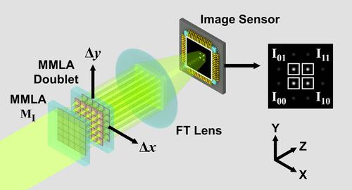
Displacement sensing with subnanometer precision is a crucial technology across various fields. There is a pressing need for a rapid, compact, long-range, and highly accurate lateral displacement measurement method that does not rely on postprocessing algorithms. In this study, we demonstrate a nanoruler based on confocal micrometalens arrays (MMLAs) for two-dimensional (2D) transverse displacement metrology. We have developed an ’optical scale’ by constructing a blazed grating with a tunable blaze angle proportional to the relative displacement between the MMLAs, enabling high-precision sensing of displacements as small as 0.5 nm when environmental noise is minimized. Our system is characterized by its simplicity and compactness, comprising only a laser, two MMLAs, a Fourier transform lens, and an image sensor. This work introduces innovative concepts for metasurface-based photonic devices and high-precision displacement metrology.
期刊介绍:
Published as soon as accepted and summarized in monthly issues, ACS Photonics will publish Research Articles, Letters, Perspectives, and Reviews, to encompass the full scope of published research in this field.


 分享
分享
 求助内容:
求助内容: 应助结果提醒方式:
 扫码关注我们
