Sjoerd Telkamp, Tommaso Antonelli, Clemens Todt, Manuel Hinderling, Marco Coraiola, Daniel Haxell, Sofieke C. ten Kate, Deividas Sabonis, Peng Zeng, Rüdiger Schott, Erik Cheah, Christian Reichl, Fabrizio Nichele, Filip Krizek, Werner Wegscheider
{"title":"Development of a Nb-Based Semiconductor-Superconductor Hybrid 2DEG Platform","authors":"Sjoerd Telkamp, Tommaso Antonelli, Clemens Todt, Manuel Hinderling, Marco Coraiola, Daniel Haxell, Sofieke C. ten Kate, Deividas Sabonis, Peng Zeng, Rüdiger Schott, Erik Cheah, Christian Reichl, Fabrizio Nichele, Filip Krizek, Werner Wegscheider","doi":"10.1002/aelm.202400687","DOIUrl":null,"url":null,"abstract":"<p>Semiconductor-superconductor hybrid materials are used as a platform to realize Andreev bound states, which hold great promise for quantum applications. These states require transparent interfaces between the semiconductor and superconductor, which are typically realized by in-situ deposition of an Al superconducting layer. Here a hybrid material is presented, based on an InAs 2D electron gas (2DEG) combined with in-situ deposited Nb and NbTi superconductors, which offer a larger operating range in temperature and magnetic field due to their larger superconducting gap. The inherent difficulty associated with the formation of an amorphous interface between III-V semiconductors and Nb-based superconductors is addressed by introducing a 7 nm Al interlayer. The Al interlayer provides an epitaxial connection between an in-situ magnetron sputtered Nb or NbTi thin film and a shallow InAs 2DEG. This metal-to-metal epitaxy is achieved by optimization of the material stack and results in an induced superconducting gap of approximately 1 meV, determined from transport measurements of superconductor-semiconductor Josephson junctions. This induced gap is approximately five times larger than the values reported for Al-based hybrid materials and indicates the formation of highly-transparent interfaces that are required in high-quality hybrid material platforms.</p>","PeriodicalId":110,"journal":{"name":"Advanced Electronic Materials","volume":"11 7","pages":""},"PeriodicalIF":5.3000,"publicationDate":"2025-01-15","publicationTypes":"Journal Article","fieldsOfStudy":null,"isOpenAccess":false,"openAccessPdf":"https://onlinelibrary.wiley.com/doi/epdf/10.1002/aelm.202400687","citationCount":"0","resultStr":null,"platform":"Semanticscholar","paperid":null,"PeriodicalName":"Advanced Electronic Materials","FirstCategoryId":"88","ListUrlMain":"https://advanced.onlinelibrary.wiley.com/doi/10.1002/aelm.202400687","RegionNum":2,"RegionCategory":"材料科学","ArticlePicture":[],"TitleCN":null,"AbstractTextCN":null,"PMCID":null,"EPubDate":"","PubModel":"","JCR":"Q2","JCRName":"MATERIALS SCIENCE, MULTIDISCIPLINARY","Score":null,"Total":0}
引用次数: 0
Abstract
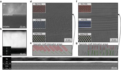
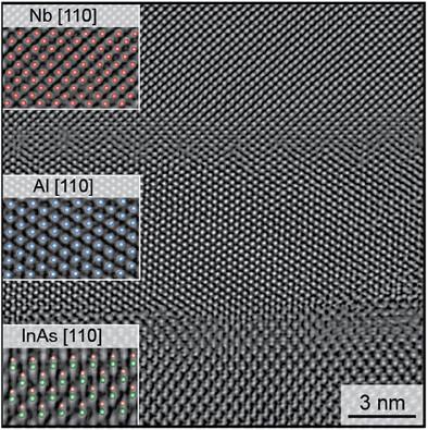
Semiconductor-superconductor hybrid materials are used as a platform to realize Andreev bound states, which hold great promise for quantum applications. These states require transparent interfaces between the semiconductor and superconductor, which are typically realized by in-situ deposition of an Al superconducting layer. Here a hybrid material is presented, based on an InAs 2D electron gas (2DEG) combined with in-situ deposited Nb and NbTi superconductors, which offer a larger operating range in temperature and magnetic field due to their larger superconducting gap. The inherent difficulty associated with the formation of an amorphous interface between III-V semiconductors and Nb-based superconductors is addressed by introducing a 7 nm Al interlayer. The Al interlayer provides an epitaxial connection between an in-situ magnetron sputtered Nb or NbTi thin film and a shallow InAs 2DEG. This metal-to-metal epitaxy is achieved by optimization of the material stack and results in an induced superconducting gap of approximately 1 meV, determined from transport measurements of superconductor-semiconductor Josephson junctions. This induced gap is approximately five times larger than the values reported for Al-based hybrid materials and indicates the formation of highly-transparent interfaces that are required in high-quality hybrid material platforms.
期刊介绍:
Advanced Electronic Materials is an interdisciplinary forum for peer-reviewed, high-quality, high-impact research in the fields of materials science, physics, and engineering of electronic and magnetic materials. It includes research on physics and physical properties of electronic and magnetic materials, spintronics, electronics, device physics and engineering, micro- and nano-electromechanical systems, and organic electronics, in addition to fundamental research.


 分享
分享
 求助内容:
求助内容: 应助结果提醒方式:
 扫码关注我们
