Anthony Cabanillas, Simran Shahi, Maomao Liu, Hemendra Nath Jaiswal, Sichen Wei, Yu Fu, Anindita Chakravarty, Asma Ahmed, Xiaochi Liu, Jian Sun, Cheng Yang, Won Jong Yoo, Theresia Knobloch, Vasili Perebeinos, Antonio Di Bartolomeo, Tibor Grasser, Fei Yao, Huamin Li
{"title":"Enormous Out-of-Plane Charge Rectification and Conductance through Two-Dimensional Monolayers","authors":"Anthony Cabanillas, Simran Shahi, Maomao Liu, Hemendra Nath Jaiswal, Sichen Wei, Yu Fu, Anindita Chakravarty, Asma Ahmed, Xiaochi Liu, Jian Sun, Cheng Yang, Won Jong Yoo, Theresia Knobloch, Vasili Perebeinos, Antonio Di Bartolomeo, Tibor Grasser, Fei Yao, Huamin Li","doi":"10.1021/acsnano.4c15271","DOIUrl":null,"url":null,"abstract":"Heterogeneous integration of emerging two-dimensional (2D) materials with mature three-dimensional (3D) silicon-based semiconductor technology presents a promising approach for the future development of energy-efficient, function-rich nanoelectronic devices. In this study, we designed a mixed-dimensional junction structure in which a 2D monolayer (e.g., graphene, MoS<sub>2</sub>, and h-BN) is sandwiched between a metal (e.g., Ti, Au, and Pd) and a 3D semiconductor (e.g., p-Si) to investigate charge transport properties exclusively in an out-of-plane (OoP) direction. The role of 2D monolayers as either an OoP metal-to-semiconductor charge injection barrier or an OoP semiconductor-to-metal charge collection barrier was comparatively evaluated. Compared to monolayer graphene, monolayer MoS<sub>2</sub> and h-BN effectively modulate OoP metal-to-semiconductor charge injection through a barrier tunneling effect. Their effective OoP resistance and resistivity were extracted using a resistors-in-series model. Intriguingly, when functioning as a semiconductor-to-metal charge collection barrier, all 2D monolayers become electronically “transparent” (close to zero resistance) when a high OoP voltage (greater than the built-in voltage) is applied. As a mixed-dimensional integrated diode, the Ti/MoS<sub>2</sub>/p-Si and Au/MoS<sub>2</sub>/p-Si configurations exhibit both high OoP rectification ratios (5.4 × 10<sup>4</sup>) and conductance (1.3 × 10<sup>5</sup> S/m<sup>2</sup>). Our work demonstrates the tunable OoP charge transport characteristics at a 2D/3D interface, suggesting the opportunity for 2D/3D heterogeneous integration, even with sub-1 nm thick 2D monolayers, to enhance modern Si-based electronic devices.","PeriodicalId":21,"journal":{"name":"ACS Nano","volume":"53 1","pages":""},"PeriodicalIF":16.0000,"publicationDate":"2025-01-15","publicationTypes":"Journal Article","fieldsOfStudy":null,"isOpenAccess":false,"openAccessPdf":"","citationCount":"0","resultStr":null,"platform":"Semanticscholar","paperid":null,"PeriodicalName":"ACS Nano","FirstCategoryId":"88","ListUrlMain":"https://doi.org/10.1021/acsnano.4c15271","RegionNum":1,"RegionCategory":"材料科学","ArticlePicture":[],"TitleCN":null,"AbstractTextCN":null,"PMCID":null,"EPubDate":"","PubModel":"","JCR":"Q1","JCRName":"CHEMISTRY, MULTIDISCIPLINARY","Score":null,"Total":0}
引用次数: 0
Abstract
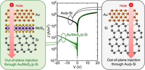
Heterogeneous integration of emerging two-dimensional (2D) materials with mature three-dimensional (3D) silicon-based semiconductor technology presents a promising approach for the future development of energy-efficient, function-rich nanoelectronic devices. In this study, we designed a mixed-dimensional junction structure in which a 2D monolayer (e.g., graphene, MoS2, and h-BN) is sandwiched between a metal (e.g., Ti, Au, and Pd) and a 3D semiconductor (e.g., p-Si) to investigate charge transport properties exclusively in an out-of-plane (OoP) direction. The role of 2D monolayers as either an OoP metal-to-semiconductor charge injection barrier or an OoP semiconductor-to-metal charge collection barrier was comparatively evaluated. Compared to monolayer graphene, monolayer MoS2 and h-BN effectively modulate OoP metal-to-semiconductor charge injection through a barrier tunneling effect. Their effective OoP resistance and resistivity were extracted using a resistors-in-series model. Intriguingly, when functioning as a semiconductor-to-metal charge collection barrier, all 2D monolayers become electronically “transparent” (close to zero resistance) when a high OoP voltage (greater than the built-in voltage) is applied. As a mixed-dimensional integrated diode, the Ti/MoS2/p-Si and Au/MoS2/p-Si configurations exhibit both high OoP rectification ratios (5.4 × 10⁴) and conductance (1.3 × 10⁵ S/m2). Our work demonstrates the tunable OoP charge transport characteristics at a 2D/3D interface, suggesting the opportunity for 2D/3D heterogeneous integration, even with sub-1 nm thick 2D monolayers, to enhance modern Si-based electronic devices.
期刊介绍:
ACS Nano, published monthly, serves as an international forum for comprehensive articles on nanoscience and nanotechnology research at the intersections of chemistry, biology, materials science, physics, and engineering. The journal fosters communication among scientists in these communities, facilitating collaboration, new research opportunities, and advancements through discoveries. ACS Nano covers synthesis, assembly, characterization, theory, and simulation of nanostructures, nanobiotechnology, nanofabrication, methods and tools for nanoscience and nanotechnology, and self- and directed-assembly. Alongside original research articles, it offers thorough reviews, perspectives on cutting-edge research, and discussions envisioning the future of nanoscience and nanotechnology.


 分享
分享
 求助内容:
求助内容: 应助结果提醒方式:
 扫码关注我们
