Kanghui Zheng, Yufeng Zhou, Ruilin Wang, Gang Wang, Qiaomu Xie, Yonghua Wang, Lin Zheng, Ganhua Fu, Jingong Pan, Shou Peng
{"title":"Rational Design and Optimization of the Band Gap and p-Type Doping in High-Efficiency CdTe Solar Cells through CuSeCN Treatment.","authors":"Kanghui Zheng, Yufeng Zhou, Ruilin Wang, Gang Wang, Qiaomu Xie, Yonghua Wang, Lin Zheng, Ganhua Fu, Jingong Pan, Shou Peng","doi":"10.1021/acsami.4c16540","DOIUrl":null,"url":null,"abstract":"<p><p>Broadening the alloyed CdSe<sub><i>x</i></sub>Te<sub>1-<i>x</i></sub> region in the absorber layer is the key to preparing highly efficient CdTe-based solar cells (SCs). With CdSe prejunction doping, the diffusion distance via the non-in situ Se doping method is restricted, and the doping ions are difficult to completely diffuse through the whole absorber layer. Moreover, the commonly used p-type back contact material CuSCN shows efficient copper doping characteristics, but the S element is not an ideal doping source for the CdTe absorber. Thus, it is demanding to develop new materials with dual activation of copper and Se. In this paper, on the one hand, CuSeCN was used as a Se doping source on the back surface of the absorber to successfully form p-CdSeTe with a band gap of 1.438 eV. On the other hand, as an emerging copper-treated material, CuSeCN is able to enhance the carrier extraction rate and lower the Schottky barrier of the device, which exhibits similar hole activation performance to CuSCN. In addition, CdTe thin-film devices treated with CuSeCN exhibit higher PCEs than those of devices treated with a CuSCN/CdSe double layer. After optimizing the experimental conditions, the short current density of CuSeCN-doped CdTe thin-film solar cells increased from 28.03 to 30.02 mA/cm<sup>2</sup>, the FF increased from 58.11 to 70.06%, and the power conversion efficiency was 17.48%. These results confirmed that CuSeCN is a promising candidate for both efficient carrier doping and lowering the band gaps of CdTe-based SCs.</p>","PeriodicalId":5,"journal":{"name":"ACS Applied Materials & Interfaces","volume":" ","pages":"9207-9218"},"PeriodicalIF":8.2000,"publicationDate":"2025-02-12","publicationTypes":"Journal Article","fieldsOfStudy":null,"isOpenAccess":false,"openAccessPdf":"","citationCount":"0","resultStr":null,"platform":"Semanticscholar","paperid":null,"PeriodicalName":"ACS Applied Materials & Interfaces","FirstCategoryId":"88","ListUrlMain":"https://doi.org/10.1021/acsami.4c16540","RegionNum":2,"RegionCategory":"材料科学","ArticlePicture":[],"TitleCN":null,"AbstractTextCN":null,"PMCID":null,"EPubDate":"2025/1/31 0:00:00","PubModel":"Epub","JCR":"Q1","JCRName":"MATERIALS SCIENCE, MULTIDISCIPLINARY","Score":null,"Total":0}
引用次数: 0
Abstract
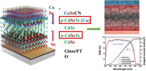
Broadening the alloyed CdSexTe1-x region in the absorber layer is the key to preparing highly efficient CdTe-based solar cells (SCs). With CdSe prejunction doping, the diffusion distance via the non-in situ Se doping method is restricted, and the doping ions are difficult to completely diffuse through the whole absorber layer. Moreover, the commonly used p-type back contact material CuSCN shows efficient copper doping characteristics, but the S element is not an ideal doping source for the CdTe absorber. Thus, it is demanding to develop new materials with dual activation of copper and Se. In this paper, on the one hand, CuSeCN was used as a Se doping source on the back surface of the absorber to successfully form p-CdSeTe with a band gap of 1.438 eV. On the other hand, as an emerging copper-treated material, CuSeCN is able to enhance the carrier extraction rate and lower the Schottky barrier of the device, which exhibits similar hole activation performance to CuSCN. In addition, CdTe thin-film devices treated with CuSeCN exhibit higher PCEs than those of devices treated with a CuSCN/CdSe double layer. After optimizing the experimental conditions, the short current density of CuSeCN-doped CdTe thin-film solar cells increased from 28.03 to 30.02 mA/cm2, the FF increased from 58.11 to 70.06%, and the power conversion efficiency was 17.48%. These results confirmed that CuSeCN is a promising candidate for both efficient carrier doping and lowering the band gaps of CdTe-based SCs.
期刊介绍:
ACS Applied Materials & Interfaces is a leading interdisciplinary journal that brings together chemists, engineers, physicists, and biologists to explore the development and utilization of newly-discovered materials and interfacial processes for specific applications. Our journal has experienced remarkable growth since its establishment in 2009, both in terms of the number of articles published and the impact of the research showcased. We are proud to foster a truly global community, with the majority of published articles originating from outside the United States, reflecting the rapid growth of applied research worldwide.


 分享
分享
 求助内容:
求助内容: 应助结果提醒方式:
 扫码关注我们
