Alfred Moore, Saqib Rafique, Ciaran Llewelyn, Dan Lamb, Lijie Li
{"title":"A Review of Ga₂O₃ Heterojunctions for Deep-UV Photodetection: Current Progress, Methodologies, and Challenges","authors":"Alfred Moore, Saqib Rafique, Ciaran Llewelyn, Dan Lamb, Lijie Li","doi":"10.1002/aelm.202400898","DOIUrl":null,"url":null,"abstract":"<p>In recent years, gallium oxide (Ga<sub>2</sub>O<sub>3</sub>) has drawn considerable research interest as an ultrawide-bandgap semiconductor due to its promising applications in the power electronics, photodetection, and gas sensing. Moreover, Ga<sub>2</sub>O<sub>3</sub> heterojunctions have emerged as a promising approach to address key limitations of Ga<sub>2</sub>O<sub>3</sub> as a standalone material—most notably, its lack of p-type doping capability. One of the key application areas for Ga<sub>2</sub>O<sub>3</sub> and its heterojunctions is ultraviolet (UV) photodetection, which has gained significant attention yet remains a relatively nascent field with vast potential for further exploration and optimization. This review provides a detailed overview of the current state-of-the-art in Ga<sub>2</sub>O<sub>3</sub> technology, highlighting recent research advancements, key challenges, and emerging strategies aimed at overcoming these challenges. Specifically, it examines Ga<sub>2</sub>O<sub>3</sub> heterojunctions for deep-UV photodetection, analysing compatible electrode materials and assessing various substrates suitable for Ga<sub>2</sub>O<sub>3</sub> growth to enhance device performance. This comprehensive review is designed to serve as an essential resource for researchers and engineers working with Ga<sub>2</sub>O<sub>3</sub>-based heterojunctions, especially for applications in UV photodetection. Written with the needs of new entrants in mind, it aims to build a robust foundational understanding of Ga<sub>2</sub>O<sub>3</sub> technology, supporting ongoing innovation and application expansion in this field.</p>","PeriodicalId":110,"journal":{"name":"Advanced Electronic Materials","volume":"11 9","pages":""},"PeriodicalIF":5.3000,"publicationDate":"2025-02-10","publicationTypes":"Journal Article","fieldsOfStudy":null,"isOpenAccess":false,"openAccessPdf":"https://onlinelibrary.wiley.com/doi/epdf/10.1002/aelm.202400898","citationCount":"0","resultStr":null,"platform":"Semanticscholar","paperid":null,"PeriodicalName":"Advanced Electronic Materials","FirstCategoryId":"88","ListUrlMain":"https://advanced.onlinelibrary.wiley.com/doi/10.1002/aelm.202400898","RegionNum":2,"RegionCategory":"材料科学","ArticlePicture":[],"TitleCN":null,"AbstractTextCN":null,"PMCID":null,"EPubDate":"","PubModel":"","JCR":"Q2","JCRName":"MATERIALS SCIENCE, MULTIDISCIPLINARY","Score":null,"Total":0}
引用次数: 0
Abstract
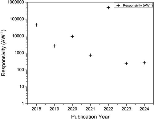
In recent years, gallium oxide (Ga2O3) has drawn considerable research interest as an ultrawide-bandgap semiconductor due to its promising applications in the power electronics, photodetection, and gas sensing. Moreover, Ga2O3 heterojunctions have emerged as a promising approach to address key limitations of Ga2O3 as a standalone material—most notably, its lack of p-type doping capability. One of the key application areas for Ga2O3 and its heterojunctions is ultraviolet (UV) photodetection, which has gained significant attention yet remains a relatively nascent field with vast potential for further exploration and optimization. This review provides a detailed overview of the current state-of-the-art in Ga2O3 technology, highlighting recent research advancements, key challenges, and emerging strategies aimed at overcoming these challenges. Specifically, it examines Ga2O3 heterojunctions for deep-UV photodetection, analysing compatible electrode materials and assessing various substrates suitable for Ga2O3 growth to enhance device performance. This comprehensive review is designed to serve as an essential resource for researchers and engineers working with Ga2O3-based heterojunctions, especially for applications in UV photodetection. Written with the needs of new entrants in mind, it aims to build a robust foundational understanding of Ga2O3 technology, supporting ongoing innovation and application expansion in this field.
期刊介绍:
Advanced Electronic Materials is an interdisciplinary forum for peer-reviewed, high-quality, high-impact research in the fields of materials science, physics, and engineering of electronic and magnetic materials. It includes research on physics and physical properties of electronic and magnetic materials, spintronics, electronics, device physics and engineering, micro- and nano-electromechanical systems, and organic electronics, in addition to fundamental research.


 分享
分享
 求助内容:
求助内容: 应助结果提醒方式:
 扫码关注我们
