{"title":"Reconfigurable Mixed-Dimensional Transistor With Semimetal CNT Contacts","authors":"Xuanzhang Li, Yuheng Li, Zhen Mei, Liang Liang, Qunqing Li, Shoushan Fan, Yang Wei","doi":"10.1002/aelm.202400782","DOIUrl":null,"url":null,"abstract":"<p>Reconfigurable low-dimensional devices are attractive for electronics in the post-Moore era. However, their performance and function design are limited by the metal–semiconductor contacts for the Fermi level pinning and fixed Schottky barrier height (SBH). Here, semimetal carbon nanotube (sCNT) contacts are incorporated into a WSe<sub>2</sub> transistor to address these issues. The transistor exhibits excellent ambipolar transfer characteristics with on/off ratio exceeding 10<sup>7</sup> for both hole and electron conduction. Furthermore, the output characteristics are reconfigured among the four equivalent modes, P–P, P–N, N–P, and N–N, by applying appropriate gate voltage. The significant forward and backward rectifying behaviors at P-N and N-P modes are highly symmetrical and have high rectification ratios of over 10<sup>6</sup>. The improvements are attributed to specific semimetal contacts for the gate-tunable SBH and the drain-induced Schottky barrier lowering (DISBL) effect. Practical circuits include a reconfigurable filter circuit and a logic invertor have been further demonstrated successfully. The progress reveals that the semimetal contacts have great potential in future reconfigurable devices and circuits.</p>","PeriodicalId":110,"journal":{"name":"Advanced Electronic Materials","volume":"11 8","pages":""},"PeriodicalIF":5.3000,"publicationDate":"2025-02-17","publicationTypes":"Journal Article","fieldsOfStudy":null,"isOpenAccess":false,"openAccessPdf":"https://onlinelibrary.wiley.com/doi/epdf/10.1002/aelm.202400782","citationCount":"0","resultStr":null,"platform":"Semanticscholar","paperid":null,"PeriodicalName":"Advanced Electronic Materials","FirstCategoryId":"88","ListUrlMain":"https://advanced.onlinelibrary.wiley.com/doi/10.1002/aelm.202400782","RegionNum":2,"RegionCategory":"材料科学","ArticlePicture":[],"TitleCN":null,"AbstractTextCN":null,"PMCID":null,"EPubDate":"","PubModel":"","JCR":"Q2","JCRName":"MATERIALS SCIENCE, MULTIDISCIPLINARY","Score":null,"Total":0}
引用次数: 0
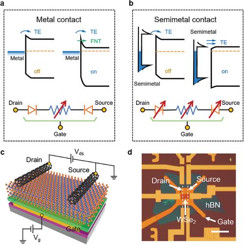
Abstract
Reconfigurable low-dimensional devices are attractive for electronics in the post-Moore era. However, their performance and function design are limited by the metal–semiconductor contacts for the Fermi level pinning and fixed Schottky barrier height (SBH). Here, semimetal carbon nanotube (sCNT) contacts are incorporated into a WSe2 transistor to address these issues. The transistor exhibits excellent ambipolar transfer characteristics with on/off ratio exceeding 107 for both hole and electron conduction. Furthermore, the output characteristics are reconfigured among the four equivalent modes, P–P, P–N, N–P, and N–N, by applying appropriate gate voltage. The significant forward and backward rectifying behaviors at P-N and N-P modes are highly symmetrical and have high rectification ratios of over 106. The improvements are attributed to specific semimetal contacts for the gate-tunable SBH and the drain-induced Schottky barrier lowering (DISBL) effect. Practical circuits include a reconfigurable filter circuit and a logic invertor have been further demonstrated successfully. The progress reveals that the semimetal contacts have great potential in future reconfigurable devices and circuits.
期刊介绍:
Advanced Electronic Materials is an interdisciplinary forum for peer-reviewed, high-quality, high-impact research in the fields of materials science, physics, and engineering of electronic and magnetic materials. It includes research on physics and physical properties of electronic and magnetic materials, spintronics, electronics, device physics and engineering, micro- and nano-electromechanical systems, and organic electronics, in addition to fundamental research.


 分享
分享
 求助内容:
求助内容: 应助结果提醒方式:
 扫码关注我们
