Jan L. Rieck, Marcel L. Kolster, Romar A. Avila, Mian Li, Guus Rijnders, Gertjan Koster, Thom Palstra, Roeland Huijink, Beatriz Noheda
{"title":"Ohmic Response in BiFeO3 Domain Walls by Submicron-Scale Four-Point Probe Resistance Measurements","authors":"Jan L. Rieck, Marcel L. Kolster, Romar A. Avila, Mian Li, Guus Rijnders, Gertjan Koster, Thom Palstra, Roeland Huijink, Beatriz Noheda","doi":"10.1002/aelm.202400794","DOIUrl":null,"url":null,"abstract":"<p>Conducting domain walls (DWs) hold promise for novel electronic devices. However, the electrical characterization of DWs is challenging because of their nanoscale dimensions and the large driving fields that are typically required due to the high resistance of the hosting material. Until now, lateral transport measurements of DWs have mainly been realized using lateral nano-gap electrode structures or conventional conducting atomic force microscopy (cAFM). Here, a non-destructive and lithography-free method is reported for lateral transport measurement of DWs, which is applied to BiFeO<sub>3</sub> (BFO) thin films utilizing a submicron-scale multi-point probe (MPP). Using different sets of individually biased probe tips, two- and four-point measurements can be conducted over various lateral distances with a minimum tip spacing of several hundreds of nanometers. These measurements reveal the ohmic behavior of ferroelastic/ferroelectric 71° DWs in BFO thin films and the first collinear four-point resistivity value of a single DW (free of lead and contact resistances). These findings contribute to a better understanding of DW conduction, highlighting the capability of MPPs for lateral transport measurements of materials containing conducting or even memristive nanoscale networks.</p>","PeriodicalId":110,"journal":{"name":"Advanced Electronic Materials","volume":"11 7","pages":""},"PeriodicalIF":5.3000,"publicationDate":"2025-02-21","publicationTypes":"Journal Article","fieldsOfStudy":null,"isOpenAccess":false,"openAccessPdf":"https://onlinelibrary.wiley.com/doi/epdf/10.1002/aelm.202400794","citationCount":"0","resultStr":null,"platform":"Semanticscholar","paperid":null,"PeriodicalName":"Advanced Electronic Materials","FirstCategoryId":"88","ListUrlMain":"https://advanced.onlinelibrary.wiley.com/doi/10.1002/aelm.202400794","RegionNum":2,"RegionCategory":"材料科学","ArticlePicture":[],"TitleCN":null,"AbstractTextCN":null,"PMCID":null,"EPubDate":"","PubModel":"","JCR":"Q2","JCRName":"MATERIALS SCIENCE, MULTIDISCIPLINARY","Score":null,"Total":0}
引用次数: 0
Abstract
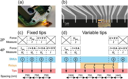
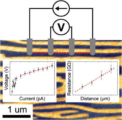
Conducting domain walls (DWs) hold promise for novel electronic devices. However, the electrical characterization of DWs is challenging because of their nanoscale dimensions and the large driving fields that are typically required due to the high resistance of the hosting material. Until now, lateral transport measurements of DWs have mainly been realized using lateral nano-gap electrode structures or conventional conducting atomic force microscopy (cAFM). Here, a non-destructive and lithography-free method is reported for lateral transport measurement of DWs, which is applied to BiFeO3 (BFO) thin films utilizing a submicron-scale multi-point probe (MPP). Using different sets of individually biased probe tips, two- and four-point measurements can be conducted over various lateral distances with a minimum tip spacing of several hundreds of nanometers. These measurements reveal the ohmic behavior of ferroelastic/ferroelectric 71° DWs in BFO thin films and the first collinear four-point resistivity value of a single DW (free of lead and contact resistances). These findings contribute to a better understanding of DW conduction, highlighting the capability of MPPs for lateral transport measurements of materials containing conducting or even memristive nanoscale networks.
期刊介绍:
Advanced Electronic Materials is an interdisciplinary forum for peer-reviewed, high-quality, high-impact research in the fields of materials science, physics, and engineering of electronic and magnetic materials. It includes research on physics and physical properties of electronic and magnetic materials, spintronics, electronics, device physics and engineering, micro- and nano-electromechanical systems, and organic electronics, in addition to fundamental research.


 分享
分享
 求助内容:
求助内容: 应助结果提醒方式:
 扫码关注我们
