Maria Elisabetta Giglio, Elisabetta Colantoni, Ilaria Fratelli, Carme Martinez-Domingo, Pedro Martinez-Zaragoza, Giulia Napolitano, Enrico Campari, Paolo Branchini, Beatrice Fraboni, Laura Basiricó, Luca Tortora, Marta Mas-Torrent
{"title":"Vertical Phase Separation in Blended Organic Semiconducting Films and Impact on Their Electrical and Direct X-Ray Detection Properties","authors":"Maria Elisabetta Giglio, Elisabetta Colantoni, Ilaria Fratelli, Carme Martinez-Domingo, Pedro Martinez-Zaragoza, Giulia Napolitano, Enrico Campari, Paolo Branchini, Beatrice Fraboni, Laura Basiricó, Luca Tortora, Marta Mas-Torrent","doi":"10.1002/aelm.202400887","DOIUrl":null,"url":null,"abstract":"<p>Blends of small-molecule organic semiconductors (OSCs) and insulating polymers in Organic Field-Effect Transistors (OFETs) are mainly used to assist the solution-processing of OSCs, but they can also reduce interfacial charge traps due to vertical phase separation. Such charge traps are known to affect both the electrical response and radiation-induced charge collection capability in these devices. This study aims to optimize vertical phase separation in blend films of 1,4,8,11-tetramethyl-6,13-triethylsilylethynyl pentacene (TMTES) and polystyrene (PS) to minimize charge trap density at the semiconductor/dielectric interface, thereby enhancing the electrical performance and direct X-ray detection sensitivity in OFETs. A PS mass concentration of 33% is identified as optimal for achieving high-quality phase separation and favorable film morphology. This formulation led to films with reduced interfacial hole trap density and improved electrical and detection capacity, demonstrating a hole field-effect mobility of (1.3 ± 0.4) cm<sup>2 </sup>V<sup>−1</sup> s<sup>−1</sup> and X-ray sensitivity of (5.6 ± 0.2) × 10<sup>3</sup> µC Gy<sup>−1</sup> cm<sup>−2</sup> at low applied voltages. Remarkably, the molecular weight of PS does not significantly impact vertical phase separation, thin film morphology, or electrical properties. These findings are crucial for the development of high-performance OFETs and their application as X-ray detectors.</p>","PeriodicalId":110,"journal":{"name":"Advanced Electronic Materials","volume":"11 17","pages":""},"PeriodicalIF":5.3000,"publicationDate":"2025-03-02","publicationTypes":"Journal Article","fieldsOfStudy":null,"isOpenAccess":false,"openAccessPdf":"https://advanced.onlinelibrary.wiley.com/doi/epdf/10.1002/aelm.202400887","citationCount":"0","resultStr":null,"platform":"Semanticscholar","paperid":null,"PeriodicalName":"Advanced Electronic Materials","FirstCategoryId":"88","ListUrlMain":"https://advanced.onlinelibrary.wiley.com/doi/10.1002/aelm.202400887","RegionNum":2,"RegionCategory":"材料科学","ArticlePicture":[],"TitleCN":null,"AbstractTextCN":null,"PMCID":null,"EPubDate":"","PubModel":"","JCR":"Q2","JCRName":"MATERIALS SCIENCE, MULTIDISCIPLINARY","Score":null,"Total":0}
引用次数: 0
Abstract
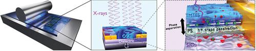
Blends of small-molecule organic semiconductors (OSCs) and insulating polymers in Organic Field-Effect Transistors (OFETs) are mainly used to assist the solution-processing of OSCs, but they can also reduce interfacial charge traps due to vertical phase separation. Such charge traps are known to affect both the electrical response and radiation-induced charge collection capability in these devices. This study aims to optimize vertical phase separation in blend films of 1,4,8,11-tetramethyl-6,13-triethylsilylethynyl pentacene (TMTES) and polystyrene (PS) to minimize charge trap density at the semiconductor/dielectric interface, thereby enhancing the electrical performance and direct X-ray detection sensitivity in OFETs. A PS mass concentration of 33% is identified as optimal for achieving high-quality phase separation and favorable film morphology. This formulation led to films with reduced interfacial hole trap density and improved electrical and detection capacity, demonstrating a hole field-effect mobility of (1.3 ± 0.4) cm2 V−1 s−1 and X-ray sensitivity of (5.6 ± 0.2) × 103 µC Gy−1 cm−2 at low applied voltages. Remarkably, the molecular weight of PS does not significantly impact vertical phase separation, thin film morphology, or electrical properties. These findings are crucial for the development of high-performance OFETs and their application as X-ray detectors.
期刊介绍:
Advanced Electronic Materials is an interdisciplinary forum for peer-reviewed, high-quality, high-impact research in the fields of materials science, physics, and engineering of electronic and magnetic materials. It includes research on physics and physical properties of electronic and magnetic materials, spintronics, electronics, device physics and engineering, micro- and nano-electromechanical systems, and organic electronics, in addition to fundamental research.


 分享
分享
 求助内容:
求助内容: 应助结果提醒方式:
 扫码关注我们
