Sophie Blundell, Thomas W. Radford, Idris A. Ajia, Daniel Lawson, Xingzhao Yan, Mehdi Banakar, David J. Thomson, Ioannis Zeimpekis, Otto L. Muskens
{"title":"Ultracompact Programmable Silicon Photonics Using Layers of Low-Loss Phase-Change Material Sb2Se3 of Increasing Thickness","authors":"Sophie Blundell, Thomas W. Radford, Idris A. Ajia, Daniel Lawson, Xingzhao Yan, Mehdi Banakar, David J. Thomson, Ioannis Zeimpekis, Otto L. Muskens","doi":"10.1021/acsphotonics.4c01789","DOIUrl":null,"url":null,"abstract":"High-performance programmable silicon photonic circuits are considered to be a critical part of next-generation architectures for optical processing, photonic quantum circuits, and neural networks. Low-loss optical phase-change materials (PCMs) offer a promising route toward nonvolatile free-form control of light. Here, we exploit the direct-write digital patterning of waveguides using layers of the PCM Sb<sub>2</sub>Se<sub>3</sub> with thickness values from 20 to 100 nm, demonstrating the scaling of induced optical phase shift with thickness and the ability to strongly increase the effect per pixel for thicker layers. We exploit the excellent refractive index matching between Sb<sub>2</sub>Se<sub>3</sub> and silicon to achieve a low-loss hybrid platform for programmable photonics. A 5-fold reduction in the modulation length of a Mach–Zehnder interferometer is achieved with increasing thickness compared to the 20 nm thin-film Sb<sub>2</sub>Se<sub>3</sub> devices, which decreased to 5 μm in this work. Application of the thicker PCM layers in direct-write digital programming of a multimode interferometer shows a corresponding 3-fold reduction of the number of programmed pixels to below 10 pixels per device. The demonstrated scaling of performance with Sb<sub>2</sub>Se<sub>3</sub> layer thickness is important for establishing the optimum working range for hybrid silicon-Sb<sub>2</sub>Se<sub>3</sub> devices and holds promise for achieving ultracompact, programmable photonic circuits.","PeriodicalId":23,"journal":{"name":"ACS Photonics","volume":"53 1","pages":""},"PeriodicalIF":6.7000,"publicationDate":"2025-03-07","publicationTypes":"Journal Article","fieldsOfStudy":null,"isOpenAccess":false,"openAccessPdf":"","citationCount":"0","resultStr":null,"platform":"Semanticscholar","paperid":null,"PeriodicalName":"ACS Photonics","FirstCategoryId":"101","ListUrlMain":"https://doi.org/10.1021/acsphotonics.4c01789","RegionNum":1,"RegionCategory":"物理与天体物理","ArticlePicture":[],"TitleCN":null,"AbstractTextCN":null,"PMCID":null,"EPubDate":"","PubModel":"","JCR":"Q1","JCRName":"MATERIALS SCIENCE, MULTIDISCIPLINARY","Score":null,"Total":0}
引用次数: 0
Abstract
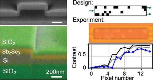
High-performance programmable silicon photonic circuits are considered to be a critical part of next-generation architectures for optical processing, photonic quantum circuits, and neural networks. Low-loss optical phase-change materials (PCMs) offer a promising route toward nonvolatile free-form control of light. Here, we exploit the direct-write digital patterning of waveguides using layers of the PCM Sb2Se3 with thickness values from 20 to 100 nm, demonstrating the scaling of induced optical phase shift with thickness and the ability to strongly increase the effect per pixel for thicker layers. We exploit the excellent refractive index matching between Sb2Se3 and silicon to achieve a low-loss hybrid platform for programmable photonics. A 5-fold reduction in the modulation length of a Mach–Zehnder interferometer is achieved with increasing thickness compared to the 20 nm thin-film Sb2Se3 devices, which decreased to 5 μm in this work. Application of the thicker PCM layers in direct-write digital programming of a multimode interferometer shows a corresponding 3-fold reduction of the number of programmed pixels to below 10 pixels per device. The demonstrated scaling of performance with Sb2Se3 layer thickness is important for establishing the optimum working range for hybrid silicon-Sb2Se3 devices and holds promise for achieving ultracompact, programmable photonic circuits.
期刊介绍:
Published as soon as accepted and summarized in monthly issues, ACS Photonics will publish Research Articles, Letters, Perspectives, and Reviews, to encompass the full scope of published research in this field.


 分享
分享
 求助内容:
求助内容: 应助结果提醒方式:
 扫码关注我们
