Tobias Wollandt, Sabrina Steffens, Yurii Radiev, Florian Letzkus, Joachim N. Burghartz, Gregor Witte, Hagen Klauk
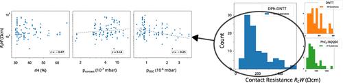
{"title":"Reliability of the Transmission Line Method and Reproducibility of the Measured Contact Resistance of Organic Thin-Film Transistors","authors":"Tobias Wollandt, Sabrina Steffens, Yurii Radiev, Florian Letzkus, Joachim N. Burghartz, Gregor Witte, Hagen Klauk","doi":"10.1021/acsnano.4c15828","DOIUrl":null,"url":null,"abstract":"Using the transmission line method (TLM), we extracted the contact resistance of organic thin-film transistors (TFTs) based on five different vacuum-deposited small-molecule semiconductors fabricated on over 500 substrates. In the first part of this report, we illustrate how the reliability of the TLM analysis is affected by the statistical uncertainty that arises from the fitting procedure and by the systematic error that is introduced if the actual channel length of the TFTs deviates from the nominal channel length. In the second part, we show that the contact resistance of organic TFTs varies significantly from one fabrication run to the next (and even across substrates fabricated within the same fabrication run), no matter how much care is taken to keep all controllable fabrication-process parameters constant. A statistical analysis reveals no strong correlations between the contact resistance and environmental parameters present during TFT fabrication, such as the humidity in the laboratory or the base pressure of the vacuum during material depositions. This suggests that the observed variation in the contact resistance is mainly stochastic. For the TFTs based on the best-performing semiconductor, the contact resistance varies between 28 Ωcm and 1 kΩcm, with a median value of 160 Ωcm.","PeriodicalId":21,"journal":{"name":"ACS Nano","volume":"53 1","pages":""},"PeriodicalIF":16.0000,"publicationDate":"2025-03-10","publicationTypes":"Journal Article","fieldsOfStudy":null,"isOpenAccess":false,"openAccessPdf":"","citationCount":"0","resultStr":null,"platform":"Semanticscholar","paperid":null,"PeriodicalName":"ACS Nano","FirstCategoryId":"88","ListUrlMain":"https://doi.org/10.1021/acsnano.4c15828","RegionNum":1,"RegionCategory":"材料科学","ArticlePicture":[],"TitleCN":null,"AbstractTextCN":null,"PMCID":null,"EPubDate":"","PubModel":"","JCR":"Q1","JCRName":"CHEMISTRY, MULTIDISCIPLINARY","Score":null,"Total":0}
引用次数: 0
Abstract
Using the transmission line method (TLM), we extracted the contact resistance of organic thin-film transistors (TFTs) based on five different vacuum-deposited small-molecule semiconductors fabricated on over 500 substrates. In the first part of this report, we illustrate how the reliability of the TLM analysis is affected by the statistical uncertainty that arises from the fitting procedure and by the systematic error that is introduced if the actual channel length of the TFTs deviates from the nominal channel length. In the second part, we show that the contact resistance of organic TFTs varies significantly from one fabrication run to the next (and even across substrates fabricated within the same fabrication run), no matter how much care is taken to keep all controllable fabrication-process parameters constant. A statistical analysis reveals no strong correlations between the contact resistance and environmental parameters present during TFT fabrication, such as the humidity in the laboratory or the base pressure of the vacuum during material depositions. This suggests that the observed variation in the contact resistance is mainly stochastic. For the TFTs based on the best-performing semiconductor, the contact resistance varies between 28 Ωcm and 1 kΩcm, with a median value of 160 Ωcm.
期刊介绍:
ACS Nano, published monthly, serves as an international forum for comprehensive articles on nanoscience and nanotechnology research at the intersections of chemistry, biology, materials science, physics, and engineering. The journal fosters communication among scientists in these communities, facilitating collaboration, new research opportunities, and advancements through discoveries. ACS Nano covers synthesis, assembly, characterization, theory, and simulation of nanostructures, nanobiotechnology, nanofabrication, methods and tools for nanoscience and nanotechnology, and self- and directed-assembly. Alongside original research articles, it offers thorough reviews, perspectives on cutting-edge research, and discussions envisioning the future of nanoscience and nanotechnology.


 分享
分享
 求助内容:
求助内容: 应助结果提醒方式:
 扫码关注我们
