{"title":"Photo-Thermal Approaches on Polyimide Film for Demonstration of Sub-50 µm Polymer Stencil Mask","authors":"Bon-Jae Koo, Jin-Hyeong Lee, Hyo-Kyung Kwon, Hwidon Lee, Joonsoo Jeong, Suk-Kyun Ahn, Min-Ho Seo","doi":"10.1002/aelm.202400979","DOIUrl":null,"url":null,"abstract":"<p>Stencil masks are widely utilized in traditional macro-scale patterning due to their simplicity and versatility in enabling various types of patterns. Compared to photoresist-based methods, stencil-based patterning enables chemical-free processing and curved surface application. However, their application to micro-scale patterning is constrained by challenges including precise fabrication, mechanical stability, and high production costs. Herein, a cost- and time-effective, single-step UV laser process is presented for fabricating polyimide stencil masks with micrometer-resolution (down to 42.4 µm feature sizes) by optimizing photothermal effects on material. Specifically, the processing conditions are systematically explored and optimized to enable efficient etching of polyimide with a UV laser while maintaining its structural stability in a glassy state. This approach successfully yielded micro-patterns with feature sizes below 50 µm on polyimide film. The developed method demonstrated high reproducibility, scalability, and stability, allowing polyimide films of varying thicknesses to be processed into stencil masks with dimensions down to 42.4 µm. Furthermore, the produced masks enable the formation of various micro-patterns, including polygonal shapes and linear features, with high aspect ratios (<1:235.8) (42.4 µm width, 10 mm length). To demonstrate the practicality of this technology, wearable motion sensors are fabricated using stencil masks and successfully applied to advanced human-machine interaction.</p>","PeriodicalId":110,"journal":{"name":"Advanced Electronic Materials","volume":"11 10","pages":""},"PeriodicalIF":5.3000,"publicationDate":"2025-04-01","publicationTypes":"Journal Article","fieldsOfStudy":null,"isOpenAccess":false,"openAccessPdf":"https://onlinelibrary.wiley.com/doi/epdf/10.1002/aelm.202400979","citationCount":"0","resultStr":null,"platform":"Semanticscholar","paperid":null,"PeriodicalName":"Advanced Electronic Materials","FirstCategoryId":"88","ListUrlMain":"https://advanced.onlinelibrary.wiley.com/doi/10.1002/aelm.202400979","RegionNum":2,"RegionCategory":"材料科学","ArticlePicture":[],"TitleCN":null,"AbstractTextCN":null,"PMCID":null,"EPubDate":"","PubModel":"","JCR":"Q2","JCRName":"MATERIALS SCIENCE, MULTIDISCIPLINARY","Score":null,"Total":0}
引用次数: 0
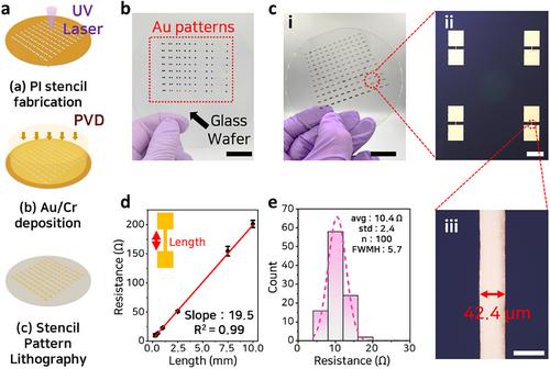
Abstract
Stencil masks are widely utilized in traditional macro-scale patterning due to their simplicity and versatility in enabling various types of patterns. Compared to photoresist-based methods, stencil-based patterning enables chemical-free processing and curved surface application. However, their application to micro-scale patterning is constrained by challenges including precise fabrication, mechanical stability, and high production costs. Herein, a cost- and time-effective, single-step UV laser process is presented for fabricating polyimide stencil masks with micrometer-resolution (down to 42.4 µm feature sizes) by optimizing photothermal effects on material. Specifically, the processing conditions are systematically explored and optimized to enable efficient etching of polyimide with a UV laser while maintaining its structural stability in a glassy state. This approach successfully yielded micro-patterns with feature sizes below 50 µm on polyimide film. The developed method demonstrated high reproducibility, scalability, and stability, allowing polyimide films of varying thicknesses to be processed into stencil masks with dimensions down to 42.4 µm. Furthermore, the produced masks enable the formation of various micro-patterns, including polygonal shapes and linear features, with high aspect ratios (<1:235.8) (42.4 µm width, 10 mm length). To demonstrate the practicality of this technology, wearable motion sensors are fabricated using stencil masks and successfully applied to advanced human-machine interaction.
期刊介绍:
Advanced Electronic Materials is an interdisciplinary forum for peer-reviewed, high-quality, high-impact research in the fields of materials science, physics, and engineering of electronic and magnetic materials. It includes research on physics and physical properties of electronic and magnetic materials, spintronics, electronics, device physics and engineering, micro- and nano-electromechanical systems, and organic electronics, in addition to fundamental research.


 分享
分享
 求助内容:
求助内容: 应助结果提醒方式:
 扫码关注我们
