Ramandeep Mandia , Mohamadali Malakoutian , Kelly Woo , Manuel A. Roldan , Srabanti Chowdhury , David J. Smith
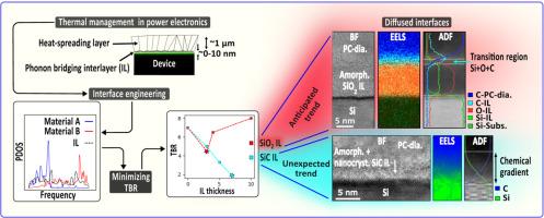
{"title":"Structural and chemical transitions in diamond/dielectric/Si heterostructures","authors":"Ramandeep Mandia , Mohamadali Malakoutian , Kelly Woo , Manuel A. Roldan , Srabanti Chowdhury , David J. Smith","doi":"10.1016/j.actamat.2025.121021","DOIUrl":null,"url":null,"abstract":"<div><div>Interfaces between polycrystalline (PC) diamond and Si substrates with thin dielectric interlayers of SiO<sub>2</sub> or SiC were studied at the atomic scale to understand the impact of the interlayer on phonon transitions from one material to the other. Our previous thermal characterization study had revealed that the dielectric interlayer led to significant reductions in the thermal boundary resistance (TBR) between diamond and Si for both interlayer types. However, the structural and chemical data needed to fully understand the underlying reason(s) for these reductions were unavailable. High-resolution scanning transmission electron microscopy and electron-energy-loss spectroscopy were used here to analyze the structural and chemical transitions within the PC-diamond/interlayer/Si heterostructures, and to correlate these observations with the trends in measured TBR values. The non-abrupt interface observed between PC-diamond and SiO<sub>2</sub> interlayers caused by intermixing of Si, C, and O during growth of the diamond layer, and the gradual changes in the Si:C ratio in SiC interlayers, appear to facilitate smooth phonon mode transitions in both cases. The SiO<sub>2</sub> interlayers exhibited the anticipated trend in TBR as a function of interlayer thickness, whereas the SiC interlayers deviated substantially from expectations, most likely due to gradual variations in the Si:C ratio and the unexpected presence of SiC nanocrystallites within the interlayer. Despite the presence of these nanocrystallites, the substantial reduction of 70 % in TBR value compared to an abrupt interface, is still significant. Overall, these results confirm that interface engineering offers a viable route towards thermal management in compact high-power electronic devices.</div></div>","PeriodicalId":238,"journal":{"name":"Acta Materialia","volume":"292 ","pages":"Article 121021"},"PeriodicalIF":9.3000,"publicationDate":"2025-06-15","publicationTypes":"Journal Article","fieldsOfStudy":null,"isOpenAccess":false,"openAccessPdf":"","citationCount":"0","resultStr":null,"platform":"Semanticscholar","paperid":null,"PeriodicalName":"Acta Materialia","FirstCategoryId":"88","ListUrlMain":"https://www.sciencedirect.com/science/article/pii/S1359645425003118","RegionNum":1,"RegionCategory":"材料科学","ArticlePicture":[],"TitleCN":null,"AbstractTextCN":null,"PMCID":null,"EPubDate":"2025/4/6 0:00:00","PubModel":"Epub","JCR":"Q1","JCRName":"MATERIALS SCIENCE, MULTIDISCIPLINARY","Score":null,"Total":0}
引用次数: 0
Abstract
Interfaces between polycrystalline (PC) diamond and Si substrates with thin dielectric interlayers of SiO2 or SiC were studied at the atomic scale to understand the impact of the interlayer on phonon transitions from one material to the other. Our previous thermal characterization study had revealed that the dielectric interlayer led to significant reductions in the thermal boundary resistance (TBR) between diamond and Si for both interlayer types. However, the structural and chemical data needed to fully understand the underlying reason(s) for these reductions were unavailable. High-resolution scanning transmission electron microscopy and electron-energy-loss spectroscopy were used here to analyze the structural and chemical transitions within the PC-diamond/interlayer/Si heterostructures, and to correlate these observations with the trends in measured TBR values. The non-abrupt interface observed between PC-diamond and SiO2 interlayers caused by intermixing of Si, C, and O during growth of the diamond layer, and the gradual changes in the Si:C ratio in SiC interlayers, appear to facilitate smooth phonon mode transitions in both cases. The SiO2 interlayers exhibited the anticipated trend in TBR as a function of interlayer thickness, whereas the SiC interlayers deviated substantially from expectations, most likely due to gradual variations in the Si:C ratio and the unexpected presence of SiC nanocrystallites within the interlayer. Despite the presence of these nanocrystallites, the substantial reduction of 70 % in TBR value compared to an abrupt interface, is still significant. Overall, these results confirm that interface engineering offers a viable route towards thermal management in compact high-power electronic devices.
期刊介绍:
Acta Materialia serves as a platform for publishing full-length, original papers and commissioned overviews that contribute to a profound understanding of the correlation between the processing, structure, and properties of inorganic materials. The journal seeks papers with high impact potential or those that significantly propel the field forward. The scope includes the atomic and molecular arrangements, chemical and electronic structures, and microstructure of materials, focusing on their mechanical or functional behavior across all length scales, including nanostructures.


 分享
分享
 求助内容:
求助内容: 应助结果提醒方式:
 扫码关注我们
