{"title":"Buried Interfacial Engineering with Potassium Hypophosphite to Suppress Ion Migration for Improved and Stabilized Perovskite Photodetectors","authors":"Jianxiang Huang, Huimin Zhang*, Huiying Zhu, Chenglin Zhang, Mingming Chen* and Dawei Cao, ","doi":"10.1021/acsaelm.5c00200","DOIUrl":null,"url":null,"abstract":"<p >As ionic crystals, halide perovskite materials have a low defect formation energy, resulting in serious ion migration. Research has shown that the density of deep-level defects near the surface of perovskites is much higher than that in the bulk. Nevertheless, up to now, many studies have focused on the top surface of perovskites, and it is rather difficult to study and passivate the buried interface defects. Here, we report an effective method for passivating the buried interface, that is, introducing potassium hypophosphite (KH<sub>2</sub>PO<sub>2</sub>) at the buried interface of perovskite, which can simultaneously regulate the crystallization of perovskite and the passivation of ionic defects. Through this strategy, the grain size of CH<sub>3</sub>NH<sub>3</sub>PbI<sub>3</sub> can be precisely controlled, high-quality thin films can be formed, and the defect density in the crystals can be reduced. By taking advantage of the reducibility of the hypophosphite ion, we can inhibit the generation of iodine and reduce metal Pb-related defects in the CH<sub>3</sub>NH<sub>3</sub>PbI<sub>3</sub> thin films. Consequently, the ionic interface charge density of the device is significantly decreased, the formation energy of ionic defects is obviously increased, and ionic migration is effectively suppressed. Finally, the performance and stability of perovskite optoelectronic devices are significantly improved.</p>","PeriodicalId":3,"journal":{"name":"ACS Applied Electronic Materials","volume":"7 7","pages":"3030–3040 3030–3040"},"PeriodicalIF":4.7000,"publicationDate":"2025-03-30","publicationTypes":"Journal Article","fieldsOfStudy":null,"isOpenAccess":false,"openAccessPdf":"","citationCount":"0","resultStr":null,"platform":"Semanticscholar","paperid":null,"PeriodicalName":"ACS Applied Electronic Materials","FirstCategoryId":"88","ListUrlMain":"https://pubs.acs.org/doi/10.1021/acsaelm.5c00200","RegionNum":3,"RegionCategory":"材料科学","ArticlePicture":[],"TitleCN":null,"AbstractTextCN":null,"PMCID":null,"EPubDate":"","PubModel":"","JCR":"Q1","JCRName":"ENGINEERING, ELECTRICAL & ELECTRONIC","Score":null,"Total":0}
引用次数: 0
Abstract
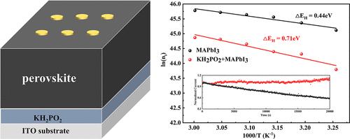
As ionic crystals, halide perovskite materials have a low defect formation energy, resulting in serious ion migration. Research has shown that the density of deep-level defects near the surface of perovskites is much higher than that in the bulk. Nevertheless, up to now, many studies have focused on the top surface of perovskites, and it is rather difficult to study and passivate the buried interface defects. Here, we report an effective method for passivating the buried interface, that is, introducing potassium hypophosphite (KH2PO2) at the buried interface of perovskite, which can simultaneously regulate the crystallization of perovskite and the passivation of ionic defects. Through this strategy, the grain size of CH3NH3PbI3 can be precisely controlled, high-quality thin films can be formed, and the defect density in the crystals can be reduced. By taking advantage of the reducibility of the hypophosphite ion, we can inhibit the generation of iodine and reduce metal Pb-related defects in the CH3NH3PbI3 thin films. Consequently, the ionic interface charge density of the device is significantly decreased, the formation energy of ionic defects is obviously increased, and ionic migration is effectively suppressed. Finally, the performance and stability of perovskite optoelectronic devices are significantly improved.
期刊介绍:
ACS Applied Electronic Materials is an interdisciplinary journal publishing original research covering all aspects of electronic materials. The journal is devoted to reports of new and original experimental and theoretical research of an applied nature that integrate knowledge in the areas of materials science, engineering, optics, physics, and chemistry into important applications of electronic materials. Sample research topics that span the journal's scope are inorganic, organic, ionic and polymeric materials with properties that include conducting, semiconducting, superconducting, insulating, dielectric, magnetic, optoelectronic, piezoelectric, ferroelectric and thermoelectric.
Indexed/Abstracted:
Web of Science SCIE
Scopus
CAS
INSPEC
Portico


 分享
分享
 求助内容:
求助内容: 应助结果提醒方式:
 扫码关注我们
