Shangfeng Liu, Tongxin Lu, Ye Yuan, Jiakang Cao, Wenting Wan, Tai Li, Tao Wang, Zhaoying Chen, Xiaoxiao Sun, Xinqiang Wang
{"title":"High Quality, Ultrathin AlN Layers with Atomically Flat Surface for Deep UV LED","authors":"Shangfeng Liu, Tongxin Lu, Ye Yuan, Jiakang Cao, Wenting Wan, Tai Li, Tao Wang, Zhaoying Chen, Xiaoxiao Sun, Xinqiang Wang","doi":"10.1002/adfm.202503580","DOIUrl":null,"url":null,"abstract":"<p>In heteroepitaxial systems with large lattice and thermal mismatches, it is extremely challenging to balance crystalline quality, surface morphology, and strain within a very limited epitaxial thickness range. Consequently, ultrathin, high-quality single-crystalline epilayers with atomically flat surfaces on hetero-substrates with large mismatches are rarely reported, as most practical devices rely on thick epitaxial templates. In this work, using AlN/sapphire as an example, high-quality, wafer-scale, ultrathin single-crystalline AlN layers on sapphire substrates are successfully achieved. These AlN layers, as thin as 50 nm, exhibit an impressively low threading dislocation density of 2.6 × 10<sup>9</sup> cm<sup>−2</sup> and a step-flow morphology. Furthermore, this novel template shows great promise for the epitaxy of deep-ultraviolet light-emitting diodes (DUV-LEDs). By optimizing strain conditions, a high-performance DUV-LED with a 150-nm-thick AlN buffer layer is demonstrated, significantly reducing the conventional requirement for an AlN thickness exceeding 2 µm. Specifically, the DUV-LED exhibits excellent performance, including a light output power of 27.8 mW and a wall-plug efficiency (WPE) of 3.95%. These achievements establish a high-quality, cost-effective, and scalable platform for III-nitride semiconductor devices, enabling advanced deep-UV optoelectronics. This breakthrough overcomes the challenge of ultrathin epitaxy on mismatched substrates while significantly reducing material usage and processing time.</p>","PeriodicalId":112,"journal":{"name":"Advanced Functional Materials","volume":"35 38","pages":""},"PeriodicalIF":19.0000,"publicationDate":"2025-04-17","publicationTypes":"Journal Article","fieldsOfStudy":null,"isOpenAccess":false,"openAccessPdf":"","citationCount":"0","resultStr":null,"platform":"Semanticscholar","paperid":null,"PeriodicalName":"Advanced Functional Materials","FirstCategoryId":"88","ListUrlMain":"https://advanced.onlinelibrary.wiley.com/doi/10.1002/adfm.202503580","RegionNum":1,"RegionCategory":"材料科学","ArticlePicture":[],"TitleCN":null,"AbstractTextCN":null,"PMCID":null,"EPubDate":"","PubModel":"","JCR":"Q1","JCRName":"CHEMISTRY, MULTIDISCIPLINARY","Score":null,"Total":0}
引用次数: 0
Abstract
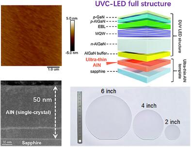
In heteroepitaxial systems with large lattice and thermal mismatches, it is extremely challenging to balance crystalline quality, surface morphology, and strain within a very limited epitaxial thickness range. Consequently, ultrathin, high-quality single-crystalline epilayers with atomically flat surfaces on hetero-substrates with large mismatches are rarely reported, as most practical devices rely on thick epitaxial templates. In this work, using AlN/sapphire as an example, high-quality, wafer-scale, ultrathin single-crystalline AlN layers on sapphire substrates are successfully achieved. These AlN layers, as thin as 50 nm, exhibit an impressively low threading dislocation density of 2.6 × 109 cm−2 and a step-flow morphology. Furthermore, this novel template shows great promise for the epitaxy of deep-ultraviolet light-emitting diodes (DUV-LEDs). By optimizing strain conditions, a high-performance DUV-LED with a 150-nm-thick AlN buffer layer is demonstrated, significantly reducing the conventional requirement for an AlN thickness exceeding 2 µm. Specifically, the DUV-LED exhibits excellent performance, including a light output power of 27.8 mW and a wall-plug efficiency (WPE) of 3.95%. These achievements establish a high-quality, cost-effective, and scalable platform for III-nitride semiconductor devices, enabling advanced deep-UV optoelectronics. This breakthrough overcomes the challenge of ultrathin epitaxy on mismatched substrates while significantly reducing material usage and processing time.
期刊介绍:
Firmly established as a top-tier materials science journal, Advanced Functional Materials reports breakthrough research in all aspects of materials science, including nanotechnology, chemistry, physics, and biology every week.
Advanced Functional Materials is known for its rapid and fair peer review, quality content, and high impact, making it the first choice of the international materials science community.


 分享
分享
 求助内容:
求助内容: 应助结果提醒方式:
 扫码关注我们
