Synergistic Control of Organic Lead Chloride Perovskite Crystallization through the Precursor and Growth Substrate for High-Performance and Stable Transparent Optoelectronics
Binchen Gong, Jinquan Lei, Yue Wang, Lingfeng Chao, Qing Song, Deli Li, Mingwei An, Yang Liu, Yang Wang, Yonghua Chen
{"title":"Synergistic Control of Organic Lead Chloride Perovskite Crystallization through the Precursor and Growth Substrate for High-Performance and Stable Transparent Optoelectronics","authors":"Binchen Gong, Jinquan Lei, Yue Wang, Lingfeng Chao, Qing Song, Deli Li, Mingwei An, Yang Liu, Yang Wang, Yonghua Chen","doi":"10.1021/acsami.5c03992","DOIUrl":null,"url":null,"abstract":"Transparent optoelectronics are crucial in modern applications, advancing display technologies in smartphones and smart windows, and supporting high-speed communication systems and advanced sensors. CH<sub>3</sub>NH<sub>3</sub>PbCl<sub>3</sub> (MAPbCl<sub>3</sub>) has garnered significant attention due to its ideal optical bandgap and outstanding optoelectronic performance. However, the fabrication of high-quality MAPbCl<sub>3</sub> thin films faces significant challenges, primarily due to the uncontrolled nucleation process, which results in nonuniform crystallization, poor surface coverage with numerous voids, and high roughness. In this work, we utilized methylammonium acetate (MAAc) as a solvent to form the MAPbCl<sub>3</sub> precursor. This approach not only enables the air-processed fabrication of MAPbCl<sub>3</sub> but also produces uniform colloidal particles, which are beneficial for the formation of compact thin films. We investigated the influence of common hole transport layers (NiO<sub><i>x</i></sub>, PTAA, PEDOT:PSS) on the crystallization of MAPbCl<sub>3</sub> films. By synergistically controlling both the precursor and the growth substrate, we significantly improved the quality of the MAPbCl<sub>3</sub> film. The resulting photodiode, based on the high-quality MAPbCl<sub>3</sub> film, demonstrated potential for transparent photovoltaics and exhibited excellent performance as a photodetector. Specifically, it achieved a responsivity <i>R</i> of 162.5 mA/W and a detectivity (<i>D*</i>) of 8.9 × 10<sup>12</sup> Jones at 390 nm, with high response speed (1.37 μs rise time and 1.68 μs fall time) even under self-powered operation (0 V). Furthermore, the device was successfully integrated into an optical communication system. These results highlight the great potential of high-quality MAPbCl<sub>3</sub> devices in transparent optoelectronic applications.","PeriodicalId":5,"journal":{"name":"ACS Applied Materials & Interfaces","volume":"33 1","pages":""},"PeriodicalIF":8.2000,"publicationDate":"2025-04-21","publicationTypes":"Journal Article","fieldsOfStudy":null,"isOpenAccess":false,"openAccessPdf":"","citationCount":"0","resultStr":null,"platform":"Semanticscholar","paperid":null,"PeriodicalName":"ACS Applied Materials & Interfaces","FirstCategoryId":"88","ListUrlMain":"https://doi.org/10.1021/acsami.5c03992","RegionNum":2,"RegionCategory":"材料科学","ArticlePicture":[],"TitleCN":null,"AbstractTextCN":null,"PMCID":null,"EPubDate":"","PubModel":"","JCR":"Q1","JCRName":"MATERIALS SCIENCE, MULTIDISCIPLINARY","Score":null,"Total":0}
引用次数: 0
Abstract
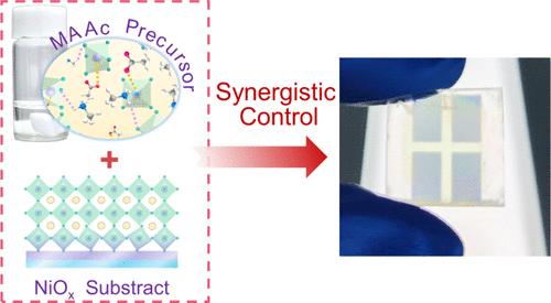
Transparent optoelectronics are crucial in modern applications, advancing display technologies in smartphones and smart windows, and supporting high-speed communication systems and advanced sensors. CH3NH3PbCl3 (MAPbCl3) has garnered significant attention due to its ideal optical bandgap and outstanding optoelectronic performance. However, the fabrication of high-quality MAPbCl3 thin films faces significant challenges, primarily due to the uncontrolled nucleation process, which results in nonuniform crystallization, poor surface coverage with numerous voids, and high roughness. In this work, we utilized methylammonium acetate (MAAc) as a solvent to form the MAPbCl3 precursor. This approach not only enables the air-processed fabrication of MAPbCl3 but also produces uniform colloidal particles, which are beneficial for the formation of compact thin films. We investigated the influence of common hole transport layers (NiOx, PTAA, PEDOT:PSS) on the crystallization of MAPbCl3 films. By synergistically controlling both the precursor and the growth substrate, we significantly improved the quality of the MAPbCl3 film. The resulting photodiode, based on the high-quality MAPbCl3 film, demonstrated potential for transparent photovoltaics and exhibited excellent performance as a photodetector. Specifically, it achieved a responsivity R of 162.5 mA/W and a detectivity (D*) of 8.9 × 10¹² Jones at 390 nm, with high response speed (1.37 μs rise time and 1.68 μs fall time) even under self-powered operation (0 V). Furthermore, the device was successfully integrated into an optical communication system. These results highlight the great potential of high-quality MAPbCl3 devices in transparent optoelectronic applications.
期刊介绍:
ACS Applied Materials & Interfaces is a leading interdisciplinary journal that brings together chemists, engineers, physicists, and biologists to explore the development and utilization of newly-discovered materials and interfacial processes for specific applications. Our journal has experienced remarkable growth since its establishment in 2009, both in terms of the number of articles published and the impact of the research showcased. We are proud to foster a truly global community, with the majority of published articles originating from outside the United States, reflecting the rapid growth of applied research worldwide.


 分享
分享
 求助内容:
求助内容: 应助结果提醒方式:
 扫码关注我们
