Ilaria Tomei, Simone Prili, Christian Petrucci, Fabrizio Arciprete, Claudio Goletti
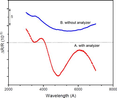
{"title":"Comment on “In-Plane Optical Anisotropy and Linear Dichroism in Low-Symmetry Layered TlSe”","authors":"Ilaria Tomei, Simone Prili, Christian Petrucci, Fabrizio Arciprete, Claudio Goletti","doi":"10.1021/acsnano.4c17053","DOIUrl":null,"url":null,"abstract":"In an article by Yang et al. (1) published in <i>ACS Nano</i>, the authors report (see Figure 3, panel d) and comment on the optical anisotropy spectrum of a chalcogenide alloy, namely, TlSe. The spectrum has been measured by a modulation optical technique there mentioned as “Azimuth-dependent reflectance difference microscopy” (ADRDM), that acquires the difference between two spectra having different and independent linearly polarized beams, modulated by a liquid crystal variable retarder. This technique is a version of reflectance anisotropy spectroscopy (RAS), (2) widely used to characterize clean surfaces in ultra high vacuum (3) and in liquid, (4) to investigate organic layers, (5) low dimensional systems, (6) and recently strain-engineered GaAsBi alloys. (7) The anisotropy spectrum reported in the article (Figure 3, panel d) is not due to the dichroism of the alloy, as instead commented by the authors: it is an artifact of the birefringence of the sample and not the result of the optical absorption of chalcogenide electronic states. Although in the paper the description of the experimental apparatus is not detailed, from the Supporting Information, it appears that reflected light after impinging on the sample surface passes again through the polarizer (see Figure S15 of ref (1)). This is more evident in another schematic diagram of the ADRDM setup, reported in the Supporting Information of a previous paper from the same group (8) (see Figure S11 of ref (8)). This configuration (with two polarizers) is the most common version of a RAS spectrometer, the so-called Aspnes version. (9) A second, rarely used version of a RAS setup (in our knowledge only two groups use also this kind of RAS spectrometer (10)) is used instead with only one polarizer (Safarov version). (10) It has been demonstrated conclusively that both versions of RAS produce the same spectra when the anisotropy in the intensity of the reflected beams is measured. (11) However, when the investigated system is birefringent (and TlSe is definitively birefringent (12)), the presence of the second polarizer (also called analyzer) produces a modulation of the light intensity that is due to the rotation of the reflected electric field and not to the absorption of the electronic states of the sample. This has been clearly demonstrated for a transparent and birefringent substrate, potassium acid phatalate (KAP): measuring an optical anisotropy spectrum in the same spectral range with (before) and without (later) an analyzer, the characteristic artifacts due to birefringence disappear completely. (13) We have then performed a new experiment on a birefringent chalcogenide sample, namely, an ordered cubic Ge<sub>2</sub>Sb<sub>2</sub>Te<sub>5</sub> alloy with (111) out of plane orientation. The 21 nm film was grown by molecular beam epitaxy (MBE) via coevaporation of ultrapure Ge, Sb, and Te on mica at a substrate temperature of 220 °C. The spectrum measured when the electric field of linearly polarized light was modulated along two orthogonal directions of the sample is reported in Figure 1 (curve A, red line), acquired by a RAS spectrometer with two polarizers. Other spectra have been recorded varying the azimuthal angle, displaying a behavior like the one reported in ref (1). At the same azimuthal angle value of spectrum A, we have then removed the analyzer and measured a new spectrum with only one polarizer: it is the blue curve in Figure 1 (curve B). As it is evident, the structures of spectrum A (well mimicking, in its waving appearance, the one reported in panel d of Figure 3, in ref (1)) have disappeared. Figure 1. RAS spectra (taken both at the same azimuthal angle, see text) of the Ge<sub>2</sub>Sb<sub>2</sub>Te<sub>5</sub> sample described in this Comment: with analyzer (curve A, red line) and without analyzer (curve B, blue line). The experimental zero line has been also reported (dotted line). RAS technique coincides with ADRDM technique mentioned in ref (1). This demonstrates that the modulation observed in Figure 3d of ref (1) is an artifact due to the configuration of the experimental ADRAM apparatus. We also comment that the labels attached by authors to maxima and minima of the spectrum in Figure 3d are incorrect. In fact, they use “E<sub>1</sub>”, “E<sub>1</sub>+Δ<sub>1</sub>”, “E<sub>2</sub>”, which is the normal way of labeling the bulk critical points for increasing photon energies. But in the figure, on the horizontal scale, wavelength values are reported; then, E<sub>2</sub> appears here at lower photon energy (higher wavelength) than E<sub>1</sub>. In addition, no calculations or published data are mentioned to strengthen this attribution to bulk critical points of TlSe. In conclusion, we have shown that the ADRAM-RAS spectrum in panel d of Figure 3 of ref (1), that has been incorrectly interpreted as due to the dichroism of bulk electronic states of the chalcogenide alloy, is due to the birefringence of TlSe. This article references 13 other publications. This article has not yet been cited by other publications.","PeriodicalId":21,"journal":{"name":"ACS Nano","volume":"1 1","pages":""},"PeriodicalIF":16.0000,"publicationDate":"2025-04-22","publicationTypes":"Journal Article","fieldsOfStudy":null,"isOpenAccess":false,"openAccessPdf":"","citationCount":"0","resultStr":null,"platform":"Semanticscholar","paperid":null,"PeriodicalName":"ACS Nano","FirstCategoryId":"88","ListUrlMain":"https://doi.org/10.1021/acsnano.4c17053","RegionNum":1,"RegionCategory":"材料科学","ArticlePicture":[],"TitleCN":null,"AbstractTextCN":null,"PMCID":null,"EPubDate":"","PubModel":"","JCR":"Q1","JCRName":"CHEMISTRY, MULTIDISCIPLINARY","Score":null,"Total":0}
引用次数: 0
Abstract
In an article by Yang et al. (1) published in ACS Nano, the authors report (see Figure 3, panel d) and comment on the optical anisotropy spectrum of a chalcogenide alloy, namely, TlSe. The spectrum has been measured by a modulation optical technique there mentioned as “Azimuth-dependent reflectance difference microscopy” (ADRDM), that acquires the difference between two spectra having different and independent linearly polarized beams, modulated by a liquid crystal variable retarder. This technique is a version of reflectance anisotropy spectroscopy (RAS), (2) widely used to characterize clean surfaces in ultra high vacuum (3) and in liquid, (4) to investigate organic layers, (5) low dimensional systems, (6) and recently strain-engineered GaAsBi alloys. (7) The anisotropy spectrum reported in the article (Figure 3, panel d) is not due to the dichroism of the alloy, as instead commented by the authors: it is an artifact of the birefringence of the sample and not the result of the optical absorption of chalcogenide electronic states. Although in the paper the description of the experimental apparatus is not detailed, from the Supporting Information, it appears that reflected light after impinging on the sample surface passes again through the polarizer (see Figure S15 of ref (1)). This is more evident in another schematic diagram of the ADRDM setup, reported in the Supporting Information of a previous paper from the same group (8) (see Figure S11 of ref (8)). This configuration (with two polarizers) is the most common version of a RAS spectrometer, the so-called Aspnes version. (9) A second, rarely used version of a RAS setup (in our knowledge only two groups use also this kind of RAS spectrometer (10)) is used instead with only one polarizer (Safarov version). (10) It has been demonstrated conclusively that both versions of RAS produce the same spectra when the anisotropy in the intensity of the reflected beams is measured. (11) However, when the investigated system is birefringent (and TlSe is definitively birefringent (12)), the presence of the second polarizer (also called analyzer) produces a modulation of the light intensity that is due to the rotation of the reflected electric field and not to the absorption of the electronic states of the sample. This has been clearly demonstrated for a transparent and birefringent substrate, potassium acid phatalate (KAP): measuring an optical anisotropy spectrum in the same spectral range with (before) and without (later) an analyzer, the characteristic artifacts due to birefringence disappear completely. (13) We have then performed a new experiment on a birefringent chalcogenide sample, namely, an ordered cubic Ge2Sb2Te5 alloy with (111) out of plane orientation. The 21 nm film was grown by molecular beam epitaxy (MBE) via coevaporation of ultrapure Ge, Sb, and Te on mica at a substrate temperature of 220 °C. The spectrum measured when the electric field of linearly polarized light was modulated along two orthogonal directions of the sample is reported in Figure 1 (curve A, red line), acquired by a RAS spectrometer with two polarizers. Other spectra have been recorded varying the azimuthal angle, displaying a behavior like the one reported in ref (1). At the same azimuthal angle value of spectrum A, we have then removed the analyzer and measured a new spectrum with only one polarizer: it is the blue curve in Figure 1 (curve B). As it is evident, the structures of spectrum A (well mimicking, in its waving appearance, the one reported in panel d of Figure 3, in ref (1)) have disappeared. Figure 1. RAS spectra (taken both at the same azimuthal angle, see text) of the Ge2Sb2Te5 sample described in this Comment: with analyzer (curve A, red line) and without analyzer (curve B, blue line). The experimental zero line has been also reported (dotted line). RAS technique coincides with ADRDM technique mentioned in ref (1). This demonstrates that the modulation observed in Figure 3d of ref (1) is an artifact due to the configuration of the experimental ADRAM apparatus. We also comment that the labels attached by authors to maxima and minima of the spectrum in Figure 3d are incorrect. In fact, they use “E1”, “E1+Δ1”, “E2”, which is the normal way of labeling the bulk critical points for increasing photon energies. But in the figure, on the horizontal scale, wavelength values are reported; then, E2 appears here at lower photon energy (higher wavelength) than E1. In addition, no calculations or published data are mentioned to strengthen this attribution to bulk critical points of TlSe. In conclusion, we have shown that the ADRAM-RAS spectrum in panel d of Figure 3 of ref (1), that has been incorrectly interpreted as due to the dichroism of bulk electronic states of the chalcogenide alloy, is due to the birefringence of TlSe. This article references 13 other publications. This article has not yet been cited by other publications.
期刊介绍:
ACS Nano, published monthly, serves as an international forum for comprehensive articles on nanoscience and nanotechnology research at the intersections of chemistry, biology, materials science, physics, and engineering. The journal fosters communication among scientists in these communities, facilitating collaboration, new research opportunities, and advancements through discoveries. ACS Nano covers synthesis, assembly, characterization, theory, and simulation of nanostructures, nanobiotechnology, nanofabrication, methods and tools for nanoscience and nanotechnology, and self- and directed-assembly. Alongside original research articles, it offers thorough reviews, perspectives on cutting-edge research, and discussions envisioning the future of nanoscience and nanotechnology.


 分享
分享
 求助内容:
求助内容: 应助结果提醒方式:
 扫码关注我们
