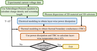
{"title":"Electrothermal properties of 2D materials in device applications","authors":"Samantha Klein, Zlatan Aksamija","doi":"10.1007/s10825-023-02091-z","DOIUrl":null,"url":null,"abstract":"<div><p>To continue downscaling transistors, new materials must be explored. Two-dimensional (2D) materials are appealing due to their thinness and bandgap. The relatively weak van der Waals forces between layers in 2D materials allow easy exfoliation and device fabrication but also result in poor heat transfer between layers and to the substrate, which is the main path for heat removal, resulting in self-heating and thermal degradation of mobility. This study explores the electrothermal properties of five popular 2D materials (MoS<sub>2</sub>, MoSe<sub>2</sub>, WS<sub>2</sub>, WSe<sub>2</sub>, and 2D black phosphorous). We simulate various devices with self-heating with a range of gate and drain biases and examine the effects on mobility and change in device temperature. The effects are compared to the isothermal case to ascertain the impact of self-heating. We observe that Joule heating has a significant effect on temperature rise, layerwise drain current, and effective mobility. We show that black phosphorous performs the best thermally, owing to its relatively high thermal conductance to the substrate, while WSe<sub>2</sub> performs the best electrically. This study will inform future thermally aware designs of nanoelectronic devices based on 2D materials.</p></div>","PeriodicalId":620,"journal":{"name":"Journal of Computational Electronics","volume":"22 5","pages":"1310 - 1318"},"PeriodicalIF":2.5000,"publicationDate":"2023-09-26","publicationTypes":"Journal Article","fieldsOfStudy":null,"isOpenAccess":false,"openAccessPdf":"https://link.springer.com/content/pdf/10.1007/s10825-023-02091-z.pdf","citationCount":"0","resultStr":null,"platform":"Semanticscholar","paperid":null,"PeriodicalName":"Journal of Computational Electronics","FirstCategoryId":"5","ListUrlMain":"https://link.springer.com/article/10.1007/s10825-023-02091-z","RegionNum":4,"RegionCategory":"工程技术","ArticlePicture":[],"TitleCN":null,"AbstractTextCN":null,"PMCID":null,"EPubDate":"","PubModel":"","JCR":"Q3","JCRName":"ENGINEERING, ELECTRICAL & ELECTRONIC","Score":null,"Total":0}
引用次数: 0
Abstract
To continue downscaling transistors, new materials must be explored. Two-dimensional (2D) materials are appealing due to their thinness and bandgap. The relatively weak van der Waals forces between layers in 2D materials allow easy exfoliation and device fabrication but also result in poor heat transfer between layers and to the substrate, which is the main path for heat removal, resulting in self-heating and thermal degradation of mobility. This study explores the electrothermal properties of five popular 2D materials (MoS2, MoSe2, WS2, WSe2, and 2D black phosphorous). We simulate various devices with self-heating with a range of gate and drain biases and examine the effects on mobility and change in device temperature. The effects are compared to the isothermal case to ascertain the impact of self-heating. We observe that Joule heating has a significant effect on temperature rise, layerwise drain current, and effective mobility. We show that black phosphorous performs the best thermally, owing to its relatively high thermal conductance to the substrate, while WSe2 performs the best electrically. This study will inform future thermally aware designs of nanoelectronic devices based on 2D materials.
期刊介绍:
he Journal of Computational Electronics brings together research on all aspects of modeling and simulation of modern electronics. This includes optical, electronic, mechanical, and quantum mechanical aspects, as well as research on the underlying mathematical algorithms and computational details. The related areas of energy conversion/storage and of molecular and biological systems, in which the thrust is on the charge transport, electronic, mechanical, and optical properties, are also covered.
In particular, we encourage manuscripts dealing with device simulation; with optical and optoelectronic systems and photonics; with energy storage (e.g. batteries, fuel cells) and harvesting (e.g. photovoltaic), with simulation of circuits, VLSI layout, logic and architecture (based on, for example, CMOS devices, quantum-cellular automata, QBITs, or single-electron transistors); with electromagnetic simulations (such as microwave electronics and components); or with molecular and biological systems. However, in all these cases, the submitted manuscripts should explicitly address the electronic properties of the relevant systems, materials, or devices and/or present novel contributions to the physical models, computational strategies, or numerical algorithms.


 分享
分享
 求助内容:
求助内容: 应助结果提醒方式:
 扫码关注我们
