Intra-level mix and match lithography with electron beam lithography and i-line stepper combined with resolution enhancement for structures below the CD-limit
C. Helke , C.H. Canpolat-Schmidt , G. Heldt , S. Schermer , S. Hartmann , A. Voigt , D. Reuter
{"title":"Intra-level mix and match lithography with electron beam lithography and i-line stepper combined with resolution enhancement for structures below the CD-limit","authors":"C. Helke , C.H. Canpolat-Schmidt , G. Heldt , S. Schermer , S. Hartmann , A. Voigt , D. Reuter","doi":"10.1016/j.mne.2023.100189","DOIUrl":null,"url":null,"abstract":"<div><p>Herein, an Intra-level Mix & Match approach (ILM&M) was investigated to combine electron beam lithography (EBL) and i-line stepper lithography on the same resist layer. This technique allows the combination of the advantages from both technologies. EBL enables the manufacturing of small sub 100 nm structures but has the disadvantage of low writing speed especially for larger structures. The i-line stepper mask- or reticle-based lithography are used for the exposure of larger features with reduced exposure time. Here the negative tone resist ma-N 1402 (from Micro Resist Technology GmbH), an UV and electrone sensitive resist was investigated in EBL and an ILM&M approach. An ILM&M process for both EBL and i-line stepper lithography is performed on the same resist layer followed by one developing step. The inspection of the developed patterns via scanning electron microscopy (SEM) showed dimensions with a 1:1 print for EBL and i-line stepper lithography with respect to the layout. By varying the exposure dose of the i-line stepper, the linear dependency to the structure width is investigated. By this means we achieved structures below the 1:1 print down to 86 nm structure width.</p></div>","PeriodicalId":37111,"journal":{"name":"Micro and Nano Engineering","volume":"19 ","pages":"Article 100189"},"PeriodicalIF":3.1000,"publicationDate":"2023-06-01","publicationTypes":"Journal Article","fieldsOfStudy":null,"isOpenAccess":false,"openAccessPdf":"","citationCount":"1","resultStr":null,"platform":"Semanticscholar","paperid":null,"PeriodicalName":"Micro and Nano Engineering","FirstCategoryId":"1085","ListUrlMain":"https://www.sciencedirect.com/science/article/pii/S2590007223000199","RegionNum":0,"RegionCategory":null,"ArticlePicture":[],"TitleCN":null,"AbstractTextCN":null,"PMCID":null,"EPubDate":"","PubModel":"","JCR":"Q2","JCRName":"ENGINEERING, ELECTRICAL & ELECTRONIC","Score":null,"Total":0}
引用次数: 1
Abstract
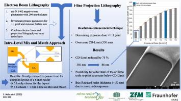
Herein, an Intra-level Mix & Match approach (ILM&M) was investigated to combine electron beam lithography (EBL) and i-line stepper lithography on the same resist layer. This technique allows the combination of the advantages from both technologies. EBL enables the manufacturing of small sub 100 nm structures but has the disadvantage of low writing speed especially for larger structures. The i-line stepper mask- or reticle-based lithography are used for the exposure of larger features with reduced exposure time. Here the negative tone resist ma-N 1402 (from Micro Resist Technology GmbH), an UV and electrone sensitive resist was investigated in EBL and an ILM&M approach. An ILM&M process for both EBL and i-line stepper lithography is performed on the same resist layer followed by one developing step. The inspection of the developed patterns via scanning electron microscopy (SEM) showed dimensions with a 1:1 print for EBL and i-line stepper lithography with respect to the layout. By varying the exposure dose of the i-line stepper, the linear dependency to the structure width is investigated. By this means we achieved structures below the 1:1 print down to 86 nm structure width.


 分享
分享
 求助内容:
求助内容: 应助结果提醒方式:
 扫码关注我们
