Byeong-Seon An, Yena Kwon, Jin-Su Oh, Yeon-Ju Shin, Jae-seon Ju, Cheol-Woong Yang
{"title":"Evaluation of ion/electron beam induced deposition for electrical connection using a modern focused ion beam system","authors":"Byeong-Seon An, Yena Kwon, Jin-Su Oh, Yeon-Ju Shin, Jae-seon Ju, Cheol-Woong Yang","doi":"10.1186/s42649-019-0008-2","DOIUrl":null,"url":null,"abstract":"<p>Focused ion beam method, which has excellent capabilities such as local deposition and selective etching, is widely used for micro-electromechanical system (MEMS)-based in situ transmission electron microscopy (TEM) sample fabrication. Among the MEMS chips in which one can apply various external stimuli, the electrical MEMS chips require connection between the TEM sample and the electrodes in MEMS chip, and a connected deposition material with low electrical resistance is required to apply the electrical signal. Therefore, in this study, we introduce an optimized condition by comparing the electrical resistance for C-, Pt-, and W- ion beam induced deposition (IBID) at 30?kV and electron beam induced deposition (EBID) at 1 and 5?kV. The W-IBID at 30?kV with the lowest electrical resistance of about 30?Ω shows better electrical properties than C- and Pt-IBID electrodes. The W-EBID at 1?kV has lower electrical resistance than that at 5?kV; thus, confirming its potential as an electrode. Therefore, for the materials that are susceptible to ion beam damage, it is recommended to fabricate electrical connections using W-EBID at 1?kV.</p>","PeriodicalId":470,"journal":{"name":"Applied Microscopy","volume":"49 1","pages":""},"PeriodicalIF":0.0000,"publicationDate":"2019-07-18","publicationTypes":"Journal Article","fieldsOfStudy":null,"isOpenAccess":false,"openAccessPdf":"https://sci-hub-pdf.com/10.1186/s42649-019-0008-2","citationCount":"6","resultStr":null,"platform":"Semanticscholar","paperid":null,"PeriodicalName":"Applied Microscopy","FirstCategoryId":"1085","ListUrlMain":"https://link.springer.com/article/10.1186/s42649-019-0008-2","RegionNum":0,"RegionCategory":null,"ArticlePicture":[],"TitleCN":null,"AbstractTextCN":null,"PMCID":null,"EPubDate":"","PubModel":"","JCR":"Q3","JCRName":"Immunology and Microbiology","Score":null,"Total":0}
引用次数: 6
Abstract
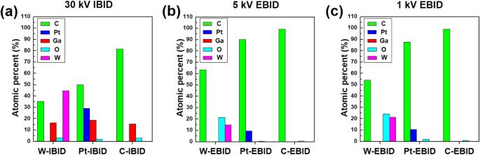
Focused ion beam method, which has excellent capabilities such as local deposition and selective etching, is widely used for micro-electromechanical system (MEMS)-based in situ transmission electron microscopy (TEM) sample fabrication. Among the MEMS chips in which one can apply various external stimuli, the electrical MEMS chips require connection between the TEM sample and the electrodes in MEMS chip, and a connected deposition material with low electrical resistance is required to apply the electrical signal. Therefore, in this study, we introduce an optimized condition by comparing the electrical resistance for C-, Pt-, and W- ion beam induced deposition (IBID) at 30?kV and electron beam induced deposition (EBID) at 1 and 5?kV. The W-IBID at 30?kV with the lowest electrical resistance of about 30?Ω shows better electrical properties than C- and Pt-IBID electrodes. The W-EBID at 1?kV has lower electrical resistance than that at 5?kV; thus, confirming its potential as an electrode. Therefore, for the materials that are susceptible to ion beam damage, it is recommended to fabricate electrical connections using W-EBID at 1?kV.
Applied MicroscopyImmunology and Microbiology-Applied Microbiology and Biotechnology
CiteScore
3.40
自引率
0.00%
发文量
10
审稿时长
10 weeks
期刊介绍:
Applied Microscopy is a peer-reviewed journal sponsored by the Korean Society of Microscopy. The journal covers all the interdisciplinary fields of technological developments in new microscopy methods and instrumentation and their applications to biological or materials science for determining structure and chemistry. ISSN: 22875123, 22874445.


 分享
分享
 求助内容:
求助内容: 应助结果提醒方式:
 扫码关注我们
