{"title":"Self-patterned ultra-sharp diamond tips and their application for advanced nanoelectronics device characterization by electrical SPM","authors":"L. Wouters, T. Boehme, L. Mana, T. Hantschel","doi":"10.1016/j.mne.2023.100195","DOIUrl":null,"url":null,"abstract":"<div><p>The continuous downscaling of nanoelectronics devices requires metrology solutions with sub-nanometer spatial resolution. Electrical scanning probe microscopy (E-SPM) techniques such as scanning spreading resistance microscopy have become important tools to map the electronic properties of these devices at nanometer scale using conductive diamond tips. Yet, the spatial resolution that can be achieved in an E-SPM measurement critically depends on the sharpness of the tip being used. Although much progress has already been made in optimizing the tip sharpness, cost-efficiently fabricated high-aspect-ratio diamond tips with ultra-high sharpness are still missing. Therefore, we have developed in this work a dry etching process for super sharp high-aspect-ratio conductive diamond tips, called hedgehog full diamond tips (HFDT), starting from standard low-aspect-ratio full diamond tips (FDT). The distinctive feature of our approach is the self-patterning etch step which benefits the high-volume production of such tips. The self-patterned mask is formed by nanoparticles originating from the interfacial layer deposited during the initial stage of the diamond growth, and metal particles from the surrounding metal cantilever material. In this work, we present our newly developed HFDTs and provide evidence that these tips outperform other conducting tips in terms of spatial resolution during E-SPM measurements.</p></div>","PeriodicalId":37111,"journal":{"name":"Micro and Nano Engineering","volume":"19 ","pages":"Article 100195"},"PeriodicalIF":3.1000,"publicationDate":"2023-06-01","publicationTypes":"Journal Article","fieldsOfStudy":null,"isOpenAccess":false,"openAccessPdf":"","citationCount":"0","resultStr":null,"platform":"Semanticscholar","paperid":null,"PeriodicalName":"Micro and Nano Engineering","FirstCategoryId":"1085","ListUrlMain":"https://www.sciencedirect.com/science/article/pii/S2590007223000254","RegionNum":0,"RegionCategory":null,"ArticlePicture":[],"TitleCN":null,"AbstractTextCN":null,"PMCID":null,"EPubDate":"","PubModel":"","JCR":"Q2","JCRName":"ENGINEERING, ELECTRICAL & ELECTRONIC","Score":null,"Total":0}
引用次数: 0
Abstract
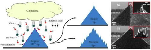
The continuous downscaling of nanoelectronics devices requires metrology solutions with sub-nanometer spatial resolution. Electrical scanning probe microscopy (E-SPM) techniques such as scanning spreading resistance microscopy have become important tools to map the electronic properties of these devices at nanometer scale using conductive diamond tips. Yet, the spatial resolution that can be achieved in an E-SPM measurement critically depends on the sharpness of the tip being used. Although much progress has already been made in optimizing the tip sharpness, cost-efficiently fabricated high-aspect-ratio diamond tips with ultra-high sharpness are still missing. Therefore, we have developed in this work a dry etching process for super sharp high-aspect-ratio conductive diamond tips, called hedgehog full diamond tips (HFDT), starting from standard low-aspect-ratio full diamond tips (FDT). The distinctive feature of our approach is the self-patterning etch step which benefits the high-volume production of such tips. The self-patterned mask is formed by nanoparticles originating from the interfacial layer deposited during the initial stage of the diamond growth, and metal particles from the surrounding metal cantilever material. In this work, we present our newly developed HFDTs and provide evidence that these tips outperform other conducting tips in terms of spatial resolution during E-SPM measurements.


 分享
分享
 求助内容:
求助内容: 应助结果提醒方式:
 扫码关注我们
