Son-Tung Nguyen, Cuong Q. Nguyen, Nguyen N. Hieu, Huynh V. Phuc and Chuong V. Nguyen
{"title":"First-principles investigations of metal–semiconductor MoSH@MoS2 van der Waals heterostructures","authors":"Son-Tung Nguyen, Cuong Q. Nguyen, Nguyen N. Hieu, Huynh V. Phuc and Chuong V. Nguyen","doi":"10.1039/D3NA00465A","DOIUrl":null,"url":null,"abstract":"<p >Two-dimensional (2D) metal–semiconductor heterostructures play a critical role in the development of modern electronics technology, offering a platform for tailored electronic behavior and enhanced device performance. Herein, we construct a novel 2D metal–semiconductor MoSH@MoS<small><sub>2</sub></small> heterostructure and investigate its structures, electronic properties and contact characteristics using first-principles investigations. We find that the MoSH@MoS<small><sub>2</sub></small> heterostructure exhibits a p-type Schottky contact, where the specific Schottky barrier height varies depending on the stacking configurations employed. Furthermore, the MoSH@MoS<small><sub>2</sub></small> heterostructures possess low tunneling probabilities, indicating a relatively low electron transparency across all the patterns of the MoSH@MoS<small><sub>2</sub></small> heterostructures. Interestingly, by modulating the electric field, it is possible to modify the Schottky barriers and achieve a transformation from a p-type Schottky contact into an n-type Schottky contact. Our findings pave the way for the development of advanced electronics technology based on metal–semiconductor MoSH@MoS<small><sub>2</sub></small> heterostructures with enhanced tunability and versatility.</p>","PeriodicalId":18806,"journal":{"name":"Nanoscale Advances","volume":" 18","pages":" 4979-4985"},"PeriodicalIF":4.6000,"publicationDate":"2023-08-17","publicationTypes":"Journal Article","fieldsOfStudy":null,"isOpenAccess":false,"openAccessPdf":"https://pubs.rsc.org/en/content/articlepdf/2023/na/d3na00465a?page=search","citationCount":"0","resultStr":null,"platform":"Semanticscholar","paperid":null,"PeriodicalName":"Nanoscale Advances","FirstCategoryId":"88","ListUrlMain":"https://pubs.rsc.org/en/content/articlelanding/2023/na/d3na00465a","RegionNum":3,"RegionCategory":"材料科学","ArticlePicture":[],"TitleCN":null,"AbstractTextCN":null,"PMCID":null,"EPubDate":"","PubModel":"","JCR":"Q2","JCRName":"CHEMISTRY, MULTIDISCIPLINARY","Score":null,"Total":0}
引用次数: 0
Abstract
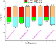
Two-dimensional (2D) metal–semiconductor heterostructures play a critical role in the development of modern electronics technology, offering a platform for tailored electronic behavior and enhanced device performance. Herein, we construct a novel 2D metal–semiconductor MoSH@MoS2 heterostructure and investigate its structures, electronic properties and contact characteristics using first-principles investigations. We find that the MoSH@MoS2 heterostructure exhibits a p-type Schottky contact, where the specific Schottky barrier height varies depending on the stacking configurations employed. Furthermore, the MoSH@MoS2 heterostructures possess low tunneling probabilities, indicating a relatively low electron transparency across all the patterns of the MoSH@MoS2 heterostructures. Interestingly, by modulating the electric field, it is possible to modify the Schottky barriers and achieve a transformation from a p-type Schottky contact into an n-type Schottky contact. Our findings pave the way for the development of advanced electronics technology based on metal–semiconductor MoSH@MoS2 heterostructures with enhanced tunability and versatility.


 分享
分享
 求助内容:
求助内容: 应助结果提醒方式:
 扫码关注我们
