C. Calabretta , V. Scuderi , C. Bongiorno , R. Anzalone , R. Reitano , A. Cannizzaro , M. Mauceri , D. Crippa , S. Boninelli , F. La Via
{"title":"Advanced approach of bulk (111) 3C-SiC epitaxial growth","authors":"C. Calabretta , V. Scuderi , C. Bongiorno , R. Anzalone , R. Reitano , A. Cannizzaro , M. Mauceri , D. Crippa , S. Boninelli , F. La Via","doi":"10.1016/j.mee.2023.112116","DOIUrl":null,"url":null,"abstract":"<div><p>3C-SiC films grown on (111) Si substrates exhibit poor crystal quality and experience wafer cracks and bowing preventing access to bulk growth. This work reports innovative Chemical Vapor Deposition (CVD) growth methodology on 4 in. Si substrates which allowed the growth of 230 mm thick layer of (111) 3C-SiC through the melting of the Si substrate in the CVD chamber and the adoption of the resulting free standing 3C-SiC for the growth of bulk (111) 3C-SiC layer under high N fluxes. From the molten KOH etching and subsequent SEM investigation it has been ascertained that with a N<sub>2</sub> flux of 1600 sccm there is a significant reduction in the concentration of stacking faults (SFs) from (7.16 ± 0.04) × 10<sup>3</sup> cm<sup>−1</sup> to (0.4 ± 0.3) × 10<sup>3</sup> cm<sup>−1</sup>. This reduction is consistent with the cross section m-PL response displaying steep and uniform increase in the intensity of the band-edge signal a factor 10 higher on the surface with respect to the equal (100) 3C-SiC grown thickness. Furthermore, the emission attributed to point defects is considerably lower in (111) 3C-SiC. From Scanning Transmission Electron Microscopy (STEM) investigation it appears evident how the typical mechanism valid in (100) growths consisting in the mutual closure of SFs coming from opposing {111} planes that give rise to Lomer and l-shaped dislocations is replaced by a different panorama of evolution. Indeed, it is shown how the SFs shred but do not interrupt each other during growth. Furthermore, dropping in the number of atomic planes composing SFs layers appears to be a key phenomenon leading to both the shrinkage of the number of SF atomic layers as well as to the SF self-closure. High Angle Annular Dark Field-Scanning Transmission Electron Microscopy (HAADF-STEM) attested how the crystal tends to smooth out the lattice mismatch until the SF is suppressed. Because of the foregoing, the mechanisms of evolution of the defects in (111) 3C-SiC revealed in this study, demonstrates how the growth parameters must be matched with the kinetics of the defects in order to endorse (111) 3C-SiC adoption in high performing devices.</p></div>","PeriodicalId":18557,"journal":{"name":"Microelectronic Engineering","volume":"283 ","pages":"Article 112116"},"PeriodicalIF":3.1000,"publicationDate":"2024-01-01","publicationTypes":"Journal Article","fieldsOfStudy":null,"isOpenAccess":false,"openAccessPdf":"https://www.sciencedirect.com/science/article/pii/S0167931723001818/pdfft?md5=db79438c2c09ef167cb61cb8c0cee2a3&pid=1-s2.0-S0167931723001818-main.pdf","citationCount":"0","resultStr":null,"platform":"Semanticscholar","paperid":null,"PeriodicalName":"Microelectronic Engineering","FirstCategoryId":"5","ListUrlMain":"https://www.sciencedirect.com/science/article/pii/S0167931723001818","RegionNum":4,"RegionCategory":"工程技术","ArticlePicture":[],"TitleCN":null,"AbstractTextCN":null,"PMCID":null,"EPubDate":"2023/10/25 0:00:00","PubModel":"Epub","JCR":"Q2","JCRName":"ENGINEERING, ELECTRICAL & ELECTRONIC","Score":null,"Total":0}
引用次数: 0
Abstract
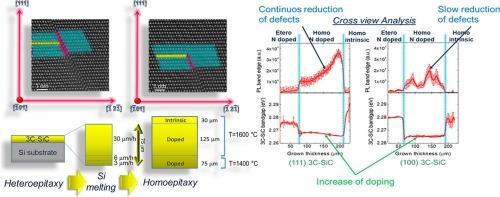
3C-SiC films grown on (111) Si substrates exhibit poor crystal quality and experience wafer cracks and bowing preventing access to bulk growth. This work reports innovative Chemical Vapor Deposition (CVD) growth methodology on 4 in. Si substrates which allowed the growth of 230 mm thick layer of (111) 3C-SiC through the melting of the Si substrate in the CVD chamber and the adoption of the resulting free standing 3C-SiC for the growth of bulk (111) 3C-SiC layer under high N fluxes. From the molten KOH etching and subsequent SEM investigation it has been ascertained that with a N2 flux of 1600 sccm there is a significant reduction in the concentration of stacking faults (SFs) from (7.16 ± 0.04) × 103 cm−1 to (0.4 ± 0.3) × 103 cm−1. This reduction is consistent with the cross section m-PL response displaying steep and uniform increase in the intensity of the band-edge signal a factor 10 higher on the surface with respect to the equal (100) 3C-SiC grown thickness. Furthermore, the emission attributed to point defects is considerably lower in (111) 3C-SiC. From Scanning Transmission Electron Microscopy (STEM) investigation it appears evident how the typical mechanism valid in (100) growths consisting in the mutual closure of SFs coming from opposing {111} planes that give rise to Lomer and l-shaped dislocations is replaced by a different panorama of evolution. Indeed, it is shown how the SFs shred but do not interrupt each other during growth. Furthermore, dropping in the number of atomic planes composing SFs layers appears to be a key phenomenon leading to both the shrinkage of the number of SF atomic layers as well as to the SF self-closure. High Angle Annular Dark Field-Scanning Transmission Electron Microscopy (HAADF-STEM) attested how the crystal tends to smooth out the lattice mismatch until the SF is suppressed. Because of the foregoing, the mechanisms of evolution of the defects in (111) 3C-SiC revealed in this study, demonstrates how the growth parameters must be matched with the kinetics of the defects in order to endorse (111) 3C-SiC adoption in high performing devices.
期刊介绍:
Microelectronic Engineering is the premier nanoprocessing, and nanotechnology journal focusing on fabrication of electronic, photonic, bioelectronic, electromechanic and fluidic devices and systems, and their applications in the broad areas of electronics, photonics, energy, life sciences, and environment. It covers also the expanding interdisciplinary field of "more than Moore" and "beyond Moore" integrated nanoelectronics / photonics and micro-/nano-/bio-systems. Through its unique mixture of peer-reviewed articles, reviews, accelerated publications, short and Technical notes, and the latest research news on key developments, Microelectronic Engineering provides comprehensive coverage of this exciting, interdisciplinary and dynamic new field for researchers in academia and professionals in industry.


 分享
分享
 求助内容:
求助内容: 应助结果提醒方式:
 扫码关注我们
