{"title":"低电流失配的模块化可编程线性电荷泵","authors":"Dimitrios Samaras, Alkiviadis Hatzopoulos","doi":"10.1007/s10470-023-02183-7","DOIUrl":null,"url":null,"abstract":"<p>In this work, a new Charge Pump (CP) design including a Phase and Frequency Detector (PFD) is presented. The PFD is designed using the common topology of two D Flip Flops, AND gates and a controllable reset delay for the DFFs to compensate for process and tem-perature variations. The Charge Pump is using a bias cell which generates the necessary bias voltages, the clock driving cells which convert the single-ended UP and DOWN signals to differential and the core cell which comprises of six slices, each one contributing the same amount of current to the low pass filter. The output current is programmable with minimum and maximum values of 25 uA and 150 uA respectively. An extra option to double the output current is also added. A new technique has been adopted in terms of layout floorplan of the charge pump slices to eliminate the clock feedthrough mismatch between the differential UP and DOWN sig-nals. The technology used in this work is TSMC 65nm, while the supply voltage is 1 V. The main characteristics of the proposed design are modularity, low power, low noise, great linearity, small area, simplicity and performance.</p>","PeriodicalId":7827,"journal":{"name":"Analog Integrated Circuits and Signal Processing","volume":"118 1","pages":"67 - 76"},"PeriodicalIF":1.4000,"publicationDate":"2023-09-30","publicationTypes":"Journal Article","fieldsOfStudy":null,"isOpenAccess":false,"openAccessPdf":"","citationCount":"0","resultStr":"{\"title\":\"A modular programmable and linear charge pump with low current mismatch\",\"authors\":\"Dimitrios Samaras, Alkiviadis Hatzopoulos\",\"doi\":\"10.1007/s10470-023-02183-7\",\"DOIUrl\":null,\"url\":null,\"abstract\":\"<p>In this work, a new Charge Pump (CP) design including a Phase and Frequency Detector (PFD) is presented. The PFD is designed using the common topology of two D Flip Flops, AND gates and a controllable reset delay for the DFFs to compensate for process and tem-perature variations. The Charge Pump is using a bias cell which generates the necessary bias voltages, the clock driving cells which convert the single-ended UP and DOWN signals to differential and the core cell which comprises of six slices, each one contributing the same amount of current to the low pass filter. The output current is programmable with minimum and maximum values of 25 uA and 150 uA respectively. An extra option to double the output current is also added. A new technique has been adopted in terms of layout floorplan of the charge pump slices to eliminate the clock feedthrough mismatch between the differential UP and DOWN sig-nals. The technology used in this work is TSMC 65nm, while the supply voltage is 1 V. The main characteristics of the proposed design are modularity, low power, low noise, great linearity, small area, simplicity and performance.</p>\",\"PeriodicalId\":7827,\"journal\":{\"name\":\"Analog Integrated Circuits and Signal Processing\",\"volume\":\"118 1\",\"pages\":\"67 - 76\"},\"PeriodicalIF\":1.4000,\"publicationDate\":\"2023-09-30\",\"publicationTypes\":\"Journal Article\",\"fieldsOfStudy\":null,\"isOpenAccess\":false,\"openAccessPdf\":\"\",\"citationCount\":\"0\",\"resultStr\":null,\"platform\":\"Semanticscholar\",\"paperid\":null,\"PeriodicalName\":\"Analog Integrated Circuits and Signal Processing\",\"FirstCategoryId\":\"5\",\"ListUrlMain\":\"https://link.springer.com/article/10.1007/s10470-023-02183-7\",\"RegionNum\":4,\"RegionCategory\":\"工程技术\",\"ArticlePicture\":[],\"TitleCN\":null,\"AbstractTextCN\":null,\"PMCID\":null,\"EPubDate\":\"\",\"PubModel\":\"\",\"JCR\":\"Q4\",\"JCRName\":\"COMPUTER SCIENCE, HARDWARE & ARCHITECTURE\",\"Score\":null,\"Total\":0}","platform":"Semanticscholar","paperid":null,"PeriodicalName":"Analog Integrated Circuits and Signal Processing","FirstCategoryId":"5","ListUrlMain":"https://link.springer.com/article/10.1007/s10470-023-02183-7","RegionNum":4,"RegionCategory":"工程技术","ArticlePicture":[],"TitleCN":null,"AbstractTextCN":null,"PMCID":null,"EPubDate":"","PubModel":"","JCR":"Q4","JCRName":"COMPUTER SCIENCE, HARDWARE & ARCHITECTURE","Score":null,"Total":0}
引用次数: 0
摘要
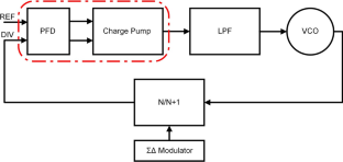
在这项工作中,介绍了一种包括相位和频率检测器 (PFD) 的新型电荷泵 (CP) 设计。PFD 采用两个 D 触发器、AND 门和 DFF 可控复位延迟的通用拓扑结构设计,以补偿工艺和温度变化。电荷泵使用一个偏置单元(产生必要的偏置电压)、时钟驱动单元(将单端上行和下行信号转换为差分信号)和核心单元(由六个片组成,每个片为低通滤波器提供相同的电流)。输出电流可编程,最小值和最大值分别为 25 uA 和 150 uA。此外,还增加了将输出电流加倍的选项。在电荷泵片的布局平面图方面采用了一种新技术,以消除差分上行和下行信号之间的时钟馈入失配。该设计的主要特点是模块化、低功耗、低噪声、高线性度、小面积、简单和高性能。
A modular programmable and linear charge pump with low current mismatch
In this work, a new Charge Pump (CP) design including a Phase and Frequency Detector (PFD) is presented. The PFD is designed using the common topology of two D Flip Flops, AND gates and a controllable reset delay for the DFFs to compensate for process and tem-perature variations. The Charge Pump is using a bias cell which generates the necessary bias voltages, the clock driving cells which convert the single-ended UP and DOWN signals to differential and the core cell which comprises of six slices, each one contributing the same amount of current to the low pass filter. The output current is programmable with minimum and maximum values of 25 uA and 150 uA respectively. An extra option to double the output current is also added. A new technique has been adopted in terms of layout floorplan of the charge pump slices to eliminate the clock feedthrough mismatch between the differential UP and DOWN sig-nals. The technology used in this work is TSMC 65nm, while the supply voltage is 1 V. The main characteristics of the proposed design are modularity, low power, low noise, great linearity, small area, simplicity and performance.
期刊介绍:
Analog Integrated Circuits and Signal Processing is an archival peer reviewed journal dedicated to the design and application of analog, radio frequency (RF), and mixed signal integrated circuits (ICs) as well as signal processing circuits and systems. It features both new research results and tutorial views and reflects the large volume of cutting-edge research activity in the worldwide field today.
A partial list of topics includes analog and mixed signal interface circuits and systems; analog and RFIC design; data converters; active-RC, switched-capacitor, and continuous-time integrated filters; mixed analog/digital VLSI systems; wireless radio transceivers; clock and data recovery circuits; and high speed optoelectronic circuits and systems.


 分享
分享
 求助内容:
求助内容: 应助结果提醒方式:
 扫码关注我们
