{"title":"用于宽带红外探测成像的界面钝化PtSe2/Ge肖特基结阵列的原位构建","authors":"Xue Li, Shuo-En Wu, Di Wu, Tianxiang Zhao, Pei Lin, Zhifeng Shi, Yongtao Tian, Xinjian Li, Longhui Zeng, Xuechao Yu","doi":"10.1002/inf2.12499","DOIUrl":null,"url":null,"abstract":"<p>Infrared (IR) detection is vital for various military and civilian applications. Recent research has highlighted the potential of two-dimensional (2D) topological semimetals in IR detection due to their distinctive advantages, including van der Waals (vdW) stacking, gapless electronic structure, and Van Hove singularities in the electronic density of states. However, challenges such as large-scale patterning, poor photoresponsivity, and high dark current of photodetectors based on 2D topological semimetals significantly impede their wider applications in low-energy photon sensing. Here, we demonstrate the in situ fabrication of PtSe<sub>2</sub>/Ge Schottky junction by directly depositing 2D PtSe<sub>2</sub> films with a vertical layer structure on a Ge substrate with an ultrathin AlO<sub>x</sub> layer. Due to high quality junction, the photodetector features a broadband response of up to 4.6 μm, along with a high specific detectivity of ~10<sup>12</sup> Jones, and operates with remarkable stability in ambient conditions as well. Moreover, the highly integrated device arrays based on PtSe<sub>2</sub>/AlO<sub>x</sub>/Ge Schottky junction showcases excellent Mid-IR (MIR) imaging capability at room temperature. These findings highlight the promising prospects of 2D topological semimetals for uncooled IR photodetection and imaging applications.</p><p>\n <figure>\n <div><picture>\n <source></source></picture><p></p>\n </div>\n </figure></p>","PeriodicalId":48538,"journal":{"name":"Infomat","volume":"6 4","pages":""},"PeriodicalIF":22.3000,"publicationDate":"2023-11-21","publicationTypes":"Journal Article","fieldsOfStudy":null,"isOpenAccess":false,"openAccessPdf":"https://onlinelibrary.wiley.com/doi/epdf/10.1002/inf2.12499","citationCount":"0","resultStr":"{\"title\":\"In situ construction of PtSe2/Ge Schottky junction array with interface passivation for broadband infrared photodetection and imaging\",\"authors\":\"Xue Li, Shuo-En Wu, Di Wu, Tianxiang Zhao, Pei Lin, Zhifeng Shi, Yongtao Tian, Xinjian Li, Longhui Zeng, Xuechao Yu\",\"doi\":\"10.1002/inf2.12499\",\"DOIUrl\":null,\"url\":null,\"abstract\":\"<p>Infrared (IR) detection is vital for various military and civilian applications. Recent research has highlighted the potential of two-dimensional (2D) topological semimetals in IR detection due to their distinctive advantages, including van der Waals (vdW) stacking, gapless electronic structure, and Van Hove singularities in the electronic density of states. However, challenges such as large-scale patterning, poor photoresponsivity, and high dark current of photodetectors based on 2D topological semimetals significantly impede their wider applications in low-energy photon sensing. Here, we demonstrate the in situ fabrication of PtSe<sub>2</sub>/Ge Schottky junction by directly depositing 2D PtSe<sub>2</sub> films with a vertical layer structure on a Ge substrate with an ultrathin AlO<sub>x</sub> layer. Due to high quality junction, the photodetector features a broadband response of up to 4.6 μm, along with a high specific detectivity of ~10<sup>12</sup> Jones, and operates with remarkable stability in ambient conditions as well. Moreover, the highly integrated device arrays based on PtSe<sub>2</sub>/AlO<sub>x</sub>/Ge Schottky junction showcases excellent Mid-IR (MIR) imaging capability at room temperature. These findings highlight the promising prospects of 2D topological semimetals for uncooled IR photodetection and imaging applications.</p><p>\\n <figure>\\n <div><picture>\\n <source></source></picture><p></p>\\n </div>\\n </figure></p>\",\"PeriodicalId\":48538,\"journal\":{\"name\":\"Infomat\",\"volume\":\"6 4\",\"pages\":\"\"},\"PeriodicalIF\":22.3000,\"publicationDate\":\"2023-11-21\",\"publicationTypes\":\"Journal Article\",\"fieldsOfStudy\":null,\"isOpenAccess\":false,\"openAccessPdf\":\"https://onlinelibrary.wiley.com/doi/epdf/10.1002/inf2.12499\",\"citationCount\":\"0\",\"resultStr\":null,\"platform\":\"Semanticscholar\",\"paperid\":null,\"PeriodicalName\":\"Infomat\",\"FirstCategoryId\":\"88\",\"ListUrlMain\":\"https://onlinelibrary.wiley.com/doi/10.1002/inf2.12499\",\"RegionNum\":1,\"RegionCategory\":\"材料科学\",\"ArticlePicture\":[],\"TitleCN\":null,\"AbstractTextCN\":null,\"PMCID\":null,\"EPubDate\":\"\",\"PubModel\":\"\",\"JCR\":\"Q1\",\"JCRName\":\"MATERIALS SCIENCE, MULTIDISCIPLINARY\",\"Score\":null,\"Total\":0}","platform":"Semanticscholar","paperid":null,"PeriodicalName":"Infomat","FirstCategoryId":"88","ListUrlMain":"https://onlinelibrary.wiley.com/doi/10.1002/inf2.12499","RegionNum":1,"RegionCategory":"材料科学","ArticlePicture":[],"TitleCN":null,"AbstractTextCN":null,"PMCID":null,"EPubDate":"","PubModel":"","JCR":"Q1","JCRName":"MATERIALS SCIENCE, MULTIDISCIPLINARY","Score":null,"Total":0}
In situ construction of PtSe2/Ge Schottky junction array with interface passivation for broadband infrared photodetection and imaging
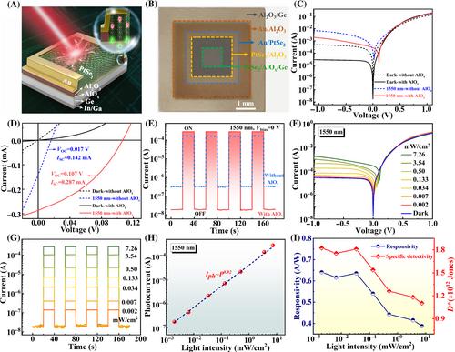
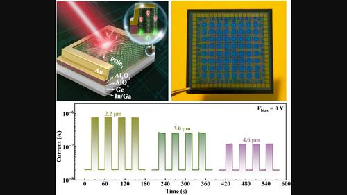
Infrared (IR) detection is vital for various military and civilian applications. Recent research has highlighted the potential of two-dimensional (2D) topological semimetals in IR detection due to their distinctive advantages, including van der Waals (vdW) stacking, gapless electronic structure, and Van Hove singularities in the electronic density of states. However, challenges such as large-scale patterning, poor photoresponsivity, and high dark current of photodetectors based on 2D topological semimetals significantly impede their wider applications in low-energy photon sensing. Here, we demonstrate the in situ fabrication of PtSe2/Ge Schottky junction by directly depositing 2D PtSe2 films with a vertical layer structure on a Ge substrate with an ultrathin AlOx layer. Due to high quality junction, the photodetector features a broadband response of up to 4.6 μm, along with a high specific detectivity of ~1012 Jones, and operates with remarkable stability in ambient conditions as well. Moreover, the highly integrated device arrays based on PtSe2/AlOx/Ge Schottky junction showcases excellent Mid-IR (MIR) imaging capability at room temperature. These findings highlight the promising prospects of 2D topological semimetals for uncooled IR photodetection and imaging applications.
期刊介绍:
InfoMat, an interdisciplinary and open-access journal, caters to the growing scientific interest in novel materials with unique electrical, optical, and magnetic properties, focusing on their applications in the rapid advancement of information technology. The journal serves as a high-quality platform for researchers across diverse scientific areas to share their findings, critical opinions, and foster collaboration between the materials science and information technology communities.


 分享
分享
 求助内容:
求助内容: 应助结果提醒方式:
 扫码关注我们
