{"title":"利用混合逻辑设计新型 1 位全加法器,实现全摆幅、面积效率和高速度","authors":"A. Arul, M. Kathirvelu","doi":"10.1007/s10470-023-02217-0","DOIUrl":null,"url":null,"abstract":"<div><p>In this research work, a novel full adder (FA) circuit is designed based on a hybrid full-swing logic with 20 transistors. The 20-transistor hybrid full-swing adder (HFSA) circuit is designed and measured based on a 12-transistor XOR–XNOR circuit, which can efficiently use chip area and power dissipation. We developed a novel 12-transistor XOR–XNOR circuit that provides glitch-free full-swing outputs. This circuit integrates 2-to-1 multiplexers, pass transistor logic, and inverters. Due to its minimum power consumption and maximum area efficiency, it is a critical component of hybrid full-swing adder circuits. This research aims to measure the efficiency and practicality of novel and eleven existing methods by considering several factors, including performance and measuring key characteristics. As a result, our novel XOR–XNOR circuit offers superior performance compared to its peers—it has a smaller chip area of 7.35 µm<sup>2</sup>, an average power of 2.44 µW, and a propagation delay (25.88 and 24.87) ps, respectively. The proposed full adder has a smaller chip area of 14.157 µm<sup>2</sup>, an average power consumption of 3.582 µW, and a propagation delay of 72.66 ps. It emphasizes large-scale structures, including 4-bit, 8-bit, 16-bit, 32-bit, and 64-bit full adders, as cascade designs utilizing a novel ripple carry adder. We also used the ADEXL design suite to analyze process corners, voltages, and temperatures, which is essential for ensuring circuit accuracy and reliability through multipoint simulations and Monte Carlo analysis. All circuits can be designed and measured in the ADEXL design suite using Cadence Virtuoso software in GPDK 45nm technology. This research shows that HFSA circuits are suitable gates for electronic component assembly. Centralized high-speed processing systems can benefit from HFSA circuits as an alternative to traditional FA circuits.</p></div>","PeriodicalId":7827,"journal":{"name":"Analog Integrated Circuits and Signal Processing","volume":"119 1","pages":"111 - 130"},"PeriodicalIF":1.2000,"publicationDate":"2023-12-29","publicationTypes":"Journal Article","fieldsOfStudy":null,"isOpenAccess":false,"openAccessPdf":"","citationCount":"0","resultStr":"{\"title\":\"Design a novel 1-bit full adder with hybrid logic for full-swing, area-efficiency and high-speed\",\"authors\":\"A. Arul, M. Kathirvelu\",\"doi\":\"10.1007/s10470-023-02217-0\",\"DOIUrl\":null,\"url\":null,\"abstract\":\"<div><p>In this research work, a novel full adder (FA) circuit is designed based on a hybrid full-swing logic with 20 transistors. The 20-transistor hybrid full-swing adder (HFSA) circuit is designed and measured based on a 12-transistor XOR–XNOR circuit, which can efficiently use chip area and power dissipation. We developed a novel 12-transistor XOR–XNOR circuit that provides glitch-free full-swing outputs. This circuit integrates 2-to-1 multiplexers, pass transistor logic, and inverters. Due to its minimum power consumption and maximum area efficiency, it is a critical component of hybrid full-swing adder circuits. This research aims to measure the efficiency and practicality of novel and eleven existing methods by considering several factors, including performance and measuring key characteristics. As a result, our novel XOR–XNOR circuit offers superior performance compared to its peers—it has a smaller chip area of 7.35 µm<sup>2</sup>, an average power of 2.44 µW, and a propagation delay (25.88 and 24.87) ps, respectively. The proposed full adder has a smaller chip area of 14.157 µm<sup>2</sup>, an average power consumption of 3.582 µW, and a propagation delay of 72.66 ps. It emphasizes large-scale structures, including 4-bit, 8-bit, 16-bit, 32-bit, and 64-bit full adders, as cascade designs utilizing a novel ripple carry adder. We also used the ADEXL design suite to analyze process corners, voltages, and temperatures, which is essential for ensuring circuit accuracy and reliability through multipoint simulations and Monte Carlo analysis. All circuits can be designed and measured in the ADEXL design suite using Cadence Virtuoso software in GPDK 45nm technology. This research shows that HFSA circuits are suitable gates for electronic component assembly. Centralized high-speed processing systems can benefit from HFSA circuits as an alternative to traditional FA circuits.</p></div>\",\"PeriodicalId\":7827,\"journal\":{\"name\":\"Analog Integrated Circuits and Signal Processing\",\"volume\":\"119 1\",\"pages\":\"111 - 130\"},\"PeriodicalIF\":1.2000,\"publicationDate\":\"2023-12-29\",\"publicationTypes\":\"Journal Article\",\"fieldsOfStudy\":null,\"isOpenAccess\":false,\"openAccessPdf\":\"\",\"citationCount\":\"0\",\"resultStr\":null,\"platform\":\"Semanticscholar\",\"paperid\":null,\"PeriodicalName\":\"Analog Integrated Circuits and Signal Processing\",\"FirstCategoryId\":\"5\",\"ListUrlMain\":\"https://link.springer.com/article/10.1007/s10470-023-02217-0\",\"RegionNum\":4,\"RegionCategory\":\"工程技术\",\"ArticlePicture\":[],\"TitleCN\":null,\"AbstractTextCN\":null,\"PMCID\":null,\"EPubDate\":\"\",\"PubModel\":\"\",\"JCR\":\"Q4\",\"JCRName\":\"COMPUTER SCIENCE, HARDWARE & ARCHITECTURE\",\"Score\":null,\"Total\":0}","platform":"Semanticscholar","paperid":null,"PeriodicalName":"Analog Integrated Circuits and Signal Processing","FirstCategoryId":"5","ListUrlMain":"https://link.springer.com/article/10.1007/s10470-023-02217-0","RegionNum":4,"RegionCategory":"工程技术","ArticlePicture":[],"TitleCN":null,"AbstractTextCN":null,"PMCID":null,"EPubDate":"","PubModel":"","JCR":"Q4","JCRName":"COMPUTER SCIENCE, HARDWARE & ARCHITECTURE","Score":null,"Total":0}
Design a novel 1-bit full adder with hybrid logic for full-swing, area-efficiency and high-speed
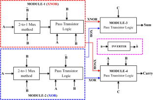
In this research work, a novel full adder (FA) circuit is designed based on a hybrid full-swing logic with 20 transistors. The 20-transistor hybrid full-swing adder (HFSA) circuit is designed and measured based on a 12-transistor XOR–XNOR circuit, which can efficiently use chip area and power dissipation. We developed a novel 12-transistor XOR–XNOR circuit that provides glitch-free full-swing outputs. This circuit integrates 2-to-1 multiplexers, pass transistor logic, and inverters. Due to its minimum power consumption and maximum area efficiency, it is a critical component of hybrid full-swing adder circuits. This research aims to measure the efficiency and practicality of novel and eleven existing methods by considering several factors, including performance and measuring key characteristics. As a result, our novel XOR–XNOR circuit offers superior performance compared to its peers—it has a smaller chip area of 7.35 µm2, an average power of 2.44 µW, and a propagation delay (25.88 and 24.87) ps, respectively. The proposed full adder has a smaller chip area of 14.157 µm2, an average power consumption of 3.582 µW, and a propagation delay of 72.66 ps. It emphasizes large-scale structures, including 4-bit, 8-bit, 16-bit, 32-bit, and 64-bit full adders, as cascade designs utilizing a novel ripple carry adder. We also used the ADEXL design suite to analyze process corners, voltages, and temperatures, which is essential for ensuring circuit accuracy and reliability through multipoint simulations and Monte Carlo analysis. All circuits can be designed and measured in the ADEXL design suite using Cadence Virtuoso software in GPDK 45nm technology. This research shows that HFSA circuits are suitable gates for electronic component assembly. Centralized high-speed processing systems can benefit from HFSA circuits as an alternative to traditional FA circuits.
期刊介绍:
Analog Integrated Circuits and Signal Processing is an archival peer reviewed journal dedicated to the design and application of analog, radio frequency (RF), and mixed signal integrated circuits (ICs) as well as signal processing circuits and systems. It features both new research results and tutorial views and reflects the large volume of cutting-edge research activity in the worldwide field today.
A partial list of topics includes analog and mixed signal interface circuits and systems; analog and RFIC design; data converters; active-RC, switched-capacitor, and continuous-time integrated filters; mixed analog/digital VLSI systems; wireless radio transceivers; clock and data recovery circuits; and high speed optoelectronic circuits and systems.


 分享
分享
 求助内容:
求助内容: 应助结果提醒方式:
 扫码关注我们
