Vitomir Sever, Nicolas Bernier, Damien Térébénec, C. Sabbione, Jessy Paterson, F. Castioni, Patrick Quéméré, A. Jannaud, J. Rouviere, Hervé Roussel, J. Raty, Françoise Hippert, Pierre Noé
{"title":"通过(准)范德华外延生长的伪二维 Sb2Te3 薄膜结构的定量 STEM HAADF 研究","authors":"Vitomir Sever, Nicolas Bernier, Damien Térébénec, C. Sabbione, Jessy Paterson, F. Castioni, Patrick Quéméré, A. Jannaud, J. Rouviere, Hervé Roussel, J. Raty, Françoise Hippert, Pierre Noé","doi":"10.1002/pssr.202300402","DOIUrl":null,"url":null,"abstract":"Scanning Transmission Electron Microscopy (STEM) techniques are used to improve our understanding of out‐of‐plane oriented Sb2Te3 thin films deposited by sputtering on SiO2 and Si substrates. Nanobeam Precession Electron Diffraction (N‐PED), Energy‐Dispersive X‐ray spectroscopy (EDX) and High‐Angle Annular Dark‐Field (HAADF) imaging show that the presence of one to two atomic planes of Te on top of the substrate is a crucial factor for successful growth of such films, which can be achieved by optimizing co‐sputtering of Te and Sb2Te3 targets. The formation of an actual van der Waals (vdW) gap between the substrate and the first Sb2Te3 quintuple layer (QL) allows for vdW epitaxy. This gap is larger than those separating Te planes in the pseudo‐2D Sb2Te3 structure. HAADF image analysis provides detailed information on the atomic arrangement such as interplanar distances, vdW gaps and Debye Waller coefficients, all these with a few pm precision. For the anisotropic atomic displacements, a new methodology is introduced based on the statiscal analysis of atomic column positions that provides information on the low‐frequency phonon modes. Ab‐initio calculations are used to support our results. Overall, this study provides quantitative STEM tools particularly well suited for non periodic pseudo‐2D materials, such as Sb2Te3/GeTe super‐lattices.This article is protected by copyright. All rights reserved.","PeriodicalId":20059,"journal":{"name":"physica status solidi (RRL) – Rapid Research Letters","volume":"7 16","pages":""},"PeriodicalIF":0.0000,"publicationDate":"2024-01-18","publicationTypes":"Journal Article","fieldsOfStudy":null,"isOpenAccess":false,"openAccessPdf":"","citationCount":"0","resultStr":"{\"title\":\"Quantitative STEM HAADF Study of the Structure of pseudo‐2D Sb2Te3 films grown by (quasi) van der Waals Epitaxy\",\"authors\":\"Vitomir Sever, Nicolas Bernier, Damien Térébénec, C. Sabbione, Jessy Paterson, F. Castioni, Patrick Quéméré, A. Jannaud, J. Rouviere, Hervé Roussel, J. Raty, Françoise Hippert, Pierre Noé\",\"doi\":\"10.1002/pssr.202300402\",\"DOIUrl\":null,\"url\":null,\"abstract\":\"Scanning Transmission Electron Microscopy (STEM) techniques are used to improve our understanding of out‐of‐plane oriented Sb2Te3 thin films deposited by sputtering on SiO2 and Si substrates. Nanobeam Precession Electron Diffraction (N‐PED), Energy‐Dispersive X‐ray spectroscopy (EDX) and High‐Angle Annular Dark‐Field (HAADF) imaging show that the presence of one to two atomic planes of Te on top of the substrate is a crucial factor for successful growth of such films, which can be achieved by optimizing co‐sputtering of Te and Sb2Te3 targets. The formation of an actual van der Waals (vdW) gap between the substrate and the first Sb2Te3 quintuple layer (QL) allows for vdW epitaxy. This gap is larger than those separating Te planes in the pseudo‐2D Sb2Te3 structure. HAADF image analysis provides detailed information on the atomic arrangement such as interplanar distances, vdW gaps and Debye Waller coefficients, all these with a few pm precision. For the anisotropic atomic displacements, a new methodology is introduced based on the statiscal analysis of atomic column positions that provides information on the low‐frequency phonon modes. Ab‐initio calculations are used to support our results. Overall, this study provides quantitative STEM tools particularly well suited for non periodic pseudo‐2D materials, such as Sb2Te3/GeTe super‐lattices.This article is protected by copyright. All rights reserved.\",\"PeriodicalId\":20059,\"journal\":{\"name\":\"physica status solidi (RRL) – Rapid Research Letters\",\"volume\":\"7 16\",\"pages\":\"\"},\"PeriodicalIF\":0.0000,\"publicationDate\":\"2024-01-18\",\"publicationTypes\":\"Journal Article\",\"fieldsOfStudy\":null,\"isOpenAccess\":false,\"openAccessPdf\":\"\",\"citationCount\":\"0\",\"resultStr\":null,\"platform\":\"Semanticscholar\",\"paperid\":null,\"PeriodicalName\":\"physica status solidi (RRL) – Rapid Research Letters\",\"FirstCategoryId\":\"1085\",\"ListUrlMain\":\"https://doi.org/10.1002/pssr.202300402\",\"RegionNum\":0,\"RegionCategory\":null,\"ArticlePicture\":[],\"TitleCN\":null,\"AbstractTextCN\":null,\"PMCID\":null,\"EPubDate\":\"\",\"PubModel\":\"\",\"JCR\":\"\",\"JCRName\":\"\",\"Score\":null,\"Total\":0}","platform":"Semanticscholar","paperid":null,"PeriodicalName":"physica status solidi (RRL) – Rapid Research Letters","FirstCategoryId":"1085","ListUrlMain":"https://doi.org/10.1002/pssr.202300402","RegionNum":0,"RegionCategory":null,"ArticlePicture":[],"TitleCN":null,"AbstractTextCN":null,"PMCID":null,"EPubDate":"","PubModel":"","JCR":"","JCRName":"","Score":null,"Total":0}
引用次数: 0
摘要
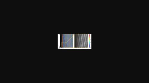
扫描透射电子显微镜(STEM)技术用于加深我们对通过溅射法沉积在二氧化硅和硅基底上的面外取向 Sb2Te3 薄膜的了解。纳米束前序电子衍射 (N-PED)、能量色散 X 射线光谱 (EDX) 和高角度环形暗场 (HAADF) 成像显示,基底顶部存在一到两个 Te 原子面是成功生长此类薄膜的关键因素,而这可以通过优化 Te 和 Sb2Te3 靶材的共溅射来实现。在基底和第一个 Sb2Te3 五重层 (QL) 之间形成一个实际的范德华 (vdW) 间隙可以实现 vdW 外延。该间隙大于伪二维 Sb2Te3 结构中 Te 平面之间的间隙。HAADF 图像分析提供了原子排列的详细信息,如平面间距、vdW 间隙和 Debye Waller 系数,所有这些信息的精度仅为几微米。对于各向异性的原子位移,引入了一种基于原子柱位置静态分析的新方法,可提供低频声子模式的信息。我们使用 Ab-initio 计算来支持我们的结果。总之,这项研究提供了定量 STEM 工具,特别适用于非周期性伪二维材料,如 Sb2Te3/GeTe 超晶格。本文受版权保护。
Quantitative STEM HAADF Study of the Structure of pseudo‐2D Sb2Te3 films grown by (quasi) van der Waals Epitaxy
Scanning Transmission Electron Microscopy (STEM) techniques are used to improve our understanding of out‐of‐plane oriented Sb2Te3 thin films deposited by sputtering on SiO2 and Si substrates. Nanobeam Precession Electron Diffraction (N‐PED), Energy‐Dispersive X‐ray spectroscopy (EDX) and High‐Angle Annular Dark‐Field (HAADF) imaging show that the presence of one to two atomic planes of Te on top of the substrate is a crucial factor for successful growth of such films, which can be achieved by optimizing co‐sputtering of Te and Sb2Te3 targets. The formation of an actual van der Waals (vdW) gap between the substrate and the first Sb2Te3 quintuple layer (QL) allows for vdW epitaxy. This gap is larger than those separating Te planes in the pseudo‐2D Sb2Te3 structure. HAADF image analysis provides detailed information on the atomic arrangement such as interplanar distances, vdW gaps and Debye Waller coefficients, all these with a few pm precision. For the anisotropic atomic displacements, a new methodology is introduced based on the statiscal analysis of atomic column positions that provides information on the low‐frequency phonon modes. Ab‐initio calculations are used to support our results. Overall, this study provides quantitative STEM tools particularly well suited for non periodic pseudo‐2D materials, such as Sb2Te3/GeTe super‐lattices.This article is protected by copyright. All rights reserved.


 分享
分享

 求助内容:
求助内容: 应助结果提醒方式:
 扫码关注我们
