Wenwu Li , Caifang Gao , Xifeng Li , Jiayan Yang , Jianhua Zhang , Junhao Chu
{"title":"掺杂铪调制氧化铟薄膜晶体管的高偏压稳定性","authors":"Wenwu Li , Caifang Gao , Xifeng Li , Jiayan Yang , Jianhua Zhang , Junhao Chu","doi":"10.1016/j.mee.2024.112142","DOIUrl":null,"url":null,"abstract":"<div><p><span>Device stability is one of the key parameters for transistor applications. To improve the stability of Indium oxide (In</span><sub>2</sub>O<sub>3</sub><span>) after a long-time gate bias, a synthetic solution of hafnium chloride (HfCl</span><sub>4</sub>) and indium nitrate (In(NO<sub>3</sub>)<sub>3</sub>∙xH<sub>2</sub>O) reagents were used to obtain 0% to 5-at.% Hf doped In<sub>2</sub>O<sub>3</sub><span><span> thin-film transistors. With the increase of Hf doping concentration, oxygen vacancies and residual hydroxyl groups continue to decrease, suppressing the carrier concentration and influencing the trap </span>state density of In</span><sub>2</sub>O<sub>3</sub>. The sub-threshold slope (SS) 0.78 V·dec<sup>−1</sup> for the undoped In<sub>2</sub>O<sub>3</sub><span> transistor in this work is a typical value. When the dopant dose is up to 5-at.%, SS decreases to 0.32 V·dec</span><sup>−1</sup><span>. According to the proportional relationship between SS and the density of trap states, it shows that the density of trap states in the dielectric layer<span> and the semiconductor/dielectric interface SS is greatly reduced after 5-at.% Hf doping. The probability of the charge being trapped is dropped as well. At the same time, under the doping of Hf, the transistor exhibits a very small threshold voltage shift. Especially at the dopant dose of 5-at.%, the transfer characteristic curve hardly shifts. This work demonstrates an In</span></span><sub>2</sub>O<sub>3</sub> transistor with high bias stability by doping method.</p></div>","PeriodicalId":18557,"journal":{"name":"Microelectronic Engineering","volume":"286 ","pages":"Article 112142"},"PeriodicalIF":3.1000,"publicationDate":"2024-03-01","publicationTypes":"Journal Article","fieldsOfStudy":null,"isOpenAccess":false,"openAccessPdf":"","citationCount":"0","resultStr":"{\"title\":\"High bias stability of Hf-doping-modulated indium oxide thin-film transistors\",\"authors\":\"Wenwu Li , Caifang Gao , Xifeng Li , Jiayan Yang , Jianhua Zhang , Junhao Chu\",\"doi\":\"10.1016/j.mee.2024.112142\",\"DOIUrl\":null,\"url\":null,\"abstract\":\"<div><p><span>Device stability is one of the key parameters for transistor applications. To improve the stability of Indium oxide (In</span><sub>2</sub>O<sub>3</sub><span>) after a long-time gate bias, a synthetic solution of hafnium chloride (HfCl</span><sub>4</sub>) and indium nitrate (In(NO<sub>3</sub>)<sub>3</sub>∙xH<sub>2</sub>O) reagents were used to obtain 0% to 5-at.% Hf doped In<sub>2</sub>O<sub>3</sub><span><span> thin-film transistors. With the increase of Hf doping concentration, oxygen vacancies and residual hydroxyl groups continue to decrease, suppressing the carrier concentration and influencing the trap </span>state density of In</span><sub>2</sub>O<sub>3</sub>. The sub-threshold slope (SS) 0.78 V·dec<sup>−1</sup> for the undoped In<sub>2</sub>O<sub>3</sub><span> transistor in this work is a typical value. When the dopant dose is up to 5-at.%, SS decreases to 0.32 V·dec</span><sup>−1</sup><span>. According to the proportional relationship between SS and the density of trap states, it shows that the density of trap states in the dielectric layer<span> and the semiconductor/dielectric interface SS is greatly reduced after 5-at.% Hf doping. The probability of the charge being trapped is dropped as well. At the same time, under the doping of Hf, the transistor exhibits a very small threshold voltage shift. Especially at the dopant dose of 5-at.%, the transfer characteristic curve hardly shifts. This work demonstrates an In</span></span><sub>2</sub>O<sub>3</sub> transistor with high bias stability by doping method.</p></div>\",\"PeriodicalId\":18557,\"journal\":{\"name\":\"Microelectronic Engineering\",\"volume\":\"286 \",\"pages\":\"Article 112142\"},\"PeriodicalIF\":3.1000,\"publicationDate\":\"2024-03-01\",\"publicationTypes\":\"Journal Article\",\"fieldsOfStudy\":null,\"isOpenAccess\":false,\"openAccessPdf\":\"\",\"citationCount\":\"0\",\"resultStr\":null,\"platform\":\"Semanticscholar\",\"paperid\":null,\"PeriodicalName\":\"Microelectronic Engineering\",\"FirstCategoryId\":\"5\",\"ListUrlMain\":\"https://www.sciencedirect.com/science/article/pii/S016793172400011X\",\"RegionNum\":4,\"RegionCategory\":\"工程技术\",\"ArticlePicture\":[],\"TitleCN\":null,\"AbstractTextCN\":null,\"PMCID\":null,\"EPubDate\":\"2024/1/22 0:00:00\",\"PubModel\":\"Epub\",\"JCR\":\"Q2\",\"JCRName\":\"ENGINEERING, ELECTRICAL & ELECTRONIC\",\"Score\":null,\"Total\":0}","platform":"Semanticscholar","paperid":null,"PeriodicalName":"Microelectronic Engineering","FirstCategoryId":"5","ListUrlMain":"https://www.sciencedirect.com/science/article/pii/S016793172400011X","RegionNum":4,"RegionCategory":"工程技术","ArticlePicture":[],"TitleCN":null,"AbstractTextCN":null,"PMCID":null,"EPubDate":"2024/1/22 0:00:00","PubModel":"Epub","JCR":"Q2","JCRName":"ENGINEERING, ELECTRICAL & ELECTRONIC","Score":null,"Total":0}
High bias stability of Hf-doping-modulated indium oxide thin-film transistors
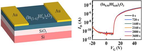
Device stability is one of the key parameters for transistor applications. To improve the stability of Indium oxide (In2O3) after a long-time gate bias, a synthetic solution of hafnium chloride (HfCl4) and indium nitrate (In(NO3)3∙xH2O) reagents were used to obtain 0% to 5-at.% Hf doped In2O3 thin-film transistors. With the increase of Hf doping concentration, oxygen vacancies and residual hydroxyl groups continue to decrease, suppressing the carrier concentration and influencing the trap state density of In2O3. The sub-threshold slope (SS) 0.78 V·dec−1 for the undoped In2O3 transistor in this work is a typical value. When the dopant dose is up to 5-at.%, SS decreases to 0.32 V·dec−1. According to the proportional relationship between SS and the density of trap states, it shows that the density of trap states in the dielectric layer and the semiconductor/dielectric interface SS is greatly reduced after 5-at.% Hf doping. The probability of the charge being trapped is dropped as well. At the same time, under the doping of Hf, the transistor exhibits a very small threshold voltage shift. Especially at the dopant dose of 5-at.%, the transfer characteristic curve hardly shifts. This work demonstrates an In2O3 transistor with high bias stability by doping method.
期刊介绍:
Microelectronic Engineering is the premier nanoprocessing, and nanotechnology journal focusing on fabrication of electronic, photonic, bioelectronic, electromechanic and fluidic devices and systems, and their applications in the broad areas of electronics, photonics, energy, life sciences, and environment. It covers also the expanding interdisciplinary field of "more than Moore" and "beyond Moore" integrated nanoelectronics / photonics and micro-/nano-/bio-systems. Through its unique mixture of peer-reviewed articles, reviews, accelerated publications, short and Technical notes, and the latest research news on key developments, Microelectronic Engineering provides comprehensive coverage of this exciting, interdisciplinary and dynamic new field for researchers in academia and professionals in industry.


 分享
分享
 求助内容:
求助内容: 应助结果提醒方式:
 扫码关注我们
