Tommaso Raveglia, Dario Crimella, Ali Gökhan Demir
{"title":"用于微电子学应用的 fs 脉冲紫外激光诱导块状铜的反向转移","authors":"Tommaso Raveglia, Dario Crimella, Ali Gökhan Demir","doi":"10.1016/j.mee.2024.112143","DOIUrl":null,"url":null,"abstract":"<div><p>Laser Induced Reverse Transfer (LIRT) is a versatile technique as a single-step deposition method allowing the localized transfer of a variety of different metals and polymers on transparent, ultra-thin and stretchable substrates. Also referred to as laser induced backward transfer (LIBT), the process can be manipulated to transfer material from bulk materials to transparent targets, providing a direct method potentially sustainable to generate microelectronic circuitry. In this work, a fs-pulsed UV laser (343 nm) was employed for the first time to transfer electrically conductive copper tracks and layers from bulk Cu in the form of sheet metal onto ultra-clear soda lime glass slides with sub-micrometric thickness. The process development started from the selection of the materials for adequate energy transfer between the beam source and the donor/receiver combination. In the single-track study, the effect of donor/receiver gap was analyzed while tracks ranges with 5 to 233 nm thickness and 7 to 41 μm average width were produced. Based on the results, multi-track layer deposition was assessed by varying the overlap between the tracks. Functional demonstrator cases were produced. The work confirms the suitability of LIRT as a direct approach to create microelectric circuitry by using readily available and sustainable bulk Cu material.</p></div>","PeriodicalId":18557,"journal":{"name":"Microelectronic Engineering","volume":"288 ","pages":"Article 112143"},"PeriodicalIF":3.3000,"publicationDate":"2024-05-01","publicationTypes":"Journal Article","fieldsOfStudy":null,"isOpenAccess":false,"openAccessPdf":"https://www.sciencedirect.com/science/article/pii/S0167931724000121/pdfft?md5=69130f80789fb89b4663a57a0e391311&pid=1-s2.0-S0167931724000121-main.pdf","citationCount":"0","resultStr":"{\"title\":\"Laser induced reverse transfer of bulk Cu with a fs-pulsed UV laser for microelectronics applications\",\"authors\":\"Tommaso Raveglia, Dario Crimella, Ali Gökhan Demir\",\"doi\":\"10.1016/j.mee.2024.112143\",\"DOIUrl\":null,\"url\":null,\"abstract\":\"<div><p>Laser Induced Reverse Transfer (LIRT) is a versatile technique as a single-step deposition method allowing the localized transfer of a variety of different metals and polymers on transparent, ultra-thin and stretchable substrates. Also referred to as laser induced backward transfer (LIBT), the process can be manipulated to transfer material from bulk materials to transparent targets, providing a direct method potentially sustainable to generate microelectronic circuitry. In this work, a fs-pulsed UV laser (343 nm) was employed for the first time to transfer electrically conductive copper tracks and layers from bulk Cu in the form of sheet metal onto ultra-clear soda lime glass slides with sub-micrometric thickness. The process development started from the selection of the materials for adequate energy transfer between the beam source and the donor/receiver combination. In the single-track study, the effect of donor/receiver gap was analyzed while tracks ranges with 5 to 233 nm thickness and 7 to 41 μm average width were produced. Based on the results, multi-track layer deposition was assessed by varying the overlap between the tracks. Functional demonstrator cases were produced. The work confirms the suitability of LIRT as a direct approach to create microelectric circuitry by using readily available and sustainable bulk Cu material.</p></div>\",\"PeriodicalId\":18557,\"journal\":{\"name\":\"Microelectronic Engineering\",\"volume\":\"288 \",\"pages\":\"Article 112143\"},\"PeriodicalIF\":3.3000,\"publicationDate\":\"2024-05-01\",\"publicationTypes\":\"Journal Article\",\"fieldsOfStudy\":null,\"isOpenAccess\":false,\"openAccessPdf\":\"https://www.sciencedirect.com/science/article/pii/S0167931724000121/pdfft?md5=69130f80789fb89b4663a57a0e391311&pid=1-s2.0-S0167931724000121-main.pdf\",\"citationCount\":\"0\",\"resultStr\":null,\"platform\":\"Semanticscholar\",\"paperid\":null,\"PeriodicalName\":\"Microelectronic Engineering\",\"FirstCategoryId\":\"5\",\"ListUrlMain\":\"https://www.sciencedirect.com/science/article/pii/S0167931724000121\",\"RegionNum\":4,\"RegionCategory\":\"工程技术\",\"ArticlePicture\":[],\"TitleCN\":null,\"AbstractTextCN\":null,\"PMCID\":null,\"EPubDate\":\"2024/1/28 0:00:00\",\"PubModel\":\"Epub\",\"JCR\":\"Q2\",\"JCRName\":\"ENGINEERING, ELECTRICAL & ELECTRONIC\",\"Score\":null,\"Total\":0}","platform":"Semanticscholar","paperid":null,"PeriodicalName":"Microelectronic Engineering","FirstCategoryId":"5","ListUrlMain":"https://www.sciencedirect.com/science/article/pii/S0167931724000121","RegionNum":4,"RegionCategory":"工程技术","ArticlePicture":[],"TitleCN":null,"AbstractTextCN":null,"PMCID":null,"EPubDate":"2024/1/28 0:00:00","PubModel":"Epub","JCR":"Q2","JCRName":"ENGINEERING, ELECTRICAL & ELECTRONIC","Score":null,"Total":0}
Laser induced reverse transfer of bulk Cu with a fs-pulsed UV laser for microelectronics applications
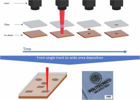
Laser Induced Reverse Transfer (LIRT) is a versatile technique as a single-step deposition method allowing the localized transfer of a variety of different metals and polymers on transparent, ultra-thin and stretchable substrates. Also referred to as laser induced backward transfer (LIBT), the process can be manipulated to transfer material from bulk materials to transparent targets, providing a direct method potentially sustainable to generate microelectronic circuitry. In this work, a fs-pulsed UV laser (343 nm) was employed for the first time to transfer electrically conductive copper tracks and layers from bulk Cu in the form of sheet metal onto ultra-clear soda lime glass slides with sub-micrometric thickness. The process development started from the selection of the materials for adequate energy transfer between the beam source and the donor/receiver combination. In the single-track study, the effect of donor/receiver gap was analyzed while tracks ranges with 5 to 233 nm thickness and 7 to 41 μm average width were produced. Based on the results, multi-track layer deposition was assessed by varying the overlap between the tracks. Functional demonstrator cases were produced. The work confirms the suitability of LIRT as a direct approach to create microelectric circuitry by using readily available and sustainable bulk Cu material.
期刊介绍:
Microelectronic Engineering is the premier nanoprocessing, and nanotechnology journal focusing on fabrication of electronic, photonic, bioelectronic, electromechanic and fluidic devices and systems, and their applications in the broad areas of electronics, photonics, energy, life sciences, and environment. It covers also the expanding interdisciplinary field of "more than Moore" and "beyond Moore" integrated nanoelectronics / photonics and micro-/nano-/bio-systems. Through its unique mixture of peer-reviewed articles, reviews, accelerated publications, short and Technical notes, and the latest research news on key developments, Microelectronic Engineering provides comprehensive coverage of this exciting, interdisciplinary and dynamic new field for researchers in academia and professionals in industry.


 分享
分享
 求助内容:
求助内容: 应助结果提醒方式:
 扫码关注我们
