{"title":"不同硼含量的电沉积硫化镉半导体薄膜的制备与表征","authors":"Erman Erdoğan","doi":"10.1002/crat.202300353","DOIUrl":null,"url":null,"abstract":"<p>In this study, Cadmium Sulfide (CdS) semiconductor films are electrodeposited on Indium Tin Oxide (ITO) substrates at 80 °C base temperature for different boric acid (H<sub>3</sub>BO<sub>3</sub>) ratios. The effect of boric acid on these films is investigated. For this, first of all, the structural change of the films is examined. Among the films obtained with different boric acid ratios, the optimum film is achieved with 0.06 <span>m</span> boric acid doped. From the basic absorption spectra (αhʋ) of the obtained CdS:B films, the variation of hʋ is drawn and it is determined that the CdS:B semiconductor films has a direct band transition. From the basic absorption spectra of the obtained CdS:B films, it is observed that the CdS:B semiconductor films has a direct band transition. In addition, the optical energy bandgap values obtained are in agreement with the values in the available literatures. The results of the structural, optical, and morphological properties of the films produced in this study indicate that among the selected additive ratios, 1% boric acid gives the best and optimum deposition condition. The thin films obtained are also found to be useful as absorber layers in photovoltaic solar cells.</p>","PeriodicalId":48935,"journal":{"name":"Crystal Research and Technology","volume":"59 6","pages":""},"PeriodicalIF":1.9000,"publicationDate":"2024-04-09","publicationTypes":"Journal Article","fieldsOfStudy":null,"isOpenAccess":false,"openAccessPdf":"","citationCount":"0","resultStr":"{\"title\":\"Production and Characterization of Electrodeposited Cadmium Sulfide Semiconductor Films with Different Boron Content\",\"authors\":\"Erman Erdoğan\",\"doi\":\"10.1002/crat.202300353\",\"DOIUrl\":null,\"url\":null,\"abstract\":\"<p>In this study, Cadmium Sulfide (CdS) semiconductor films are electrodeposited on Indium Tin Oxide (ITO) substrates at 80 °C base temperature for different boric acid (H<sub>3</sub>BO<sub>3</sub>) ratios. The effect of boric acid on these films is investigated. For this, first of all, the structural change of the films is examined. Among the films obtained with different boric acid ratios, the optimum film is achieved with 0.06 <span>m</span> boric acid doped. From the basic absorption spectra (αhʋ) of the obtained CdS:B films, the variation of hʋ is drawn and it is determined that the CdS:B semiconductor films has a direct band transition. From the basic absorption spectra of the obtained CdS:B films, it is observed that the CdS:B semiconductor films has a direct band transition. In addition, the optical energy bandgap values obtained are in agreement with the values in the available literatures. The results of the structural, optical, and morphological properties of the films produced in this study indicate that among the selected additive ratios, 1% boric acid gives the best and optimum deposition condition. The thin films obtained are also found to be useful as absorber layers in photovoltaic solar cells.</p>\",\"PeriodicalId\":48935,\"journal\":{\"name\":\"Crystal Research and Technology\",\"volume\":\"59 6\",\"pages\":\"\"},\"PeriodicalIF\":1.9000,\"publicationDate\":\"2024-04-09\",\"publicationTypes\":\"Journal Article\",\"fieldsOfStudy\":null,\"isOpenAccess\":false,\"openAccessPdf\":\"\",\"citationCount\":\"0\",\"resultStr\":null,\"platform\":\"Semanticscholar\",\"paperid\":null,\"PeriodicalName\":\"Crystal Research and Technology\",\"FirstCategoryId\":\"88\",\"ListUrlMain\":\"https://onlinelibrary.wiley.com/doi/10.1002/crat.202300353\",\"RegionNum\":4,\"RegionCategory\":\"材料科学\",\"ArticlePicture\":[],\"TitleCN\":null,\"AbstractTextCN\":null,\"PMCID\":null,\"EPubDate\":\"\",\"PubModel\":\"\",\"JCR\":\"Q3\",\"JCRName\":\"Chemistry\",\"Score\":null,\"Total\":0}","platform":"Semanticscholar","paperid":null,"PeriodicalName":"Crystal Research and Technology","FirstCategoryId":"88","ListUrlMain":"https://onlinelibrary.wiley.com/doi/10.1002/crat.202300353","RegionNum":4,"RegionCategory":"材料科学","ArticlePicture":[],"TitleCN":null,"AbstractTextCN":null,"PMCID":null,"EPubDate":"","PubModel":"","JCR":"Q3","JCRName":"Chemistry","Score":null,"Total":0}
引用次数: 0
摘要
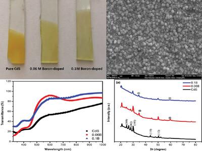
在本研究中,硫化镉(CdS)半导体薄膜是在 80 °C 基底温度下,以不同的硼酸(H3BO3)比例电沉积在氧化铟锡(ITO)基底上的。研究了硼酸对这些薄膜的影响。为此,首先考察了薄膜的结构变化。在不同硼酸比例下获得的薄膜中,掺杂 0.06 m 硼酸的薄膜效果最佳。从所得到的 CdS:B 薄膜的基本吸收光谱(αhʋ)中可以得出 hʋ 的变化,并确定 CdS:B 半导体薄膜具有直接带跃迁。从得到的 CdS:B 薄膜的基本吸收光谱可以看出,CdS:B 半导体薄膜具有直接能带跃迁。此外,所获得的光能带隙值与现有文献中的值一致。本研究中生成的薄膜的结构、光学和形态特性结果表明,在所选的添加剂比例中,1% 的硼酸给出了最佳和最优的沉积条件。获得的薄膜还可用作光伏太阳能电池的吸收层。
Production and Characterization of Electrodeposited Cadmium Sulfide Semiconductor Films with Different Boron Content
In this study, Cadmium Sulfide (CdS) semiconductor films are electrodeposited on Indium Tin Oxide (ITO) substrates at 80 °C base temperature for different boric acid (H3BO3) ratios. The effect of boric acid on these films is investigated. For this, first of all, the structural change of the films is examined. Among the films obtained with different boric acid ratios, the optimum film is achieved with 0.06 m boric acid doped. From the basic absorption spectra (αhʋ) of the obtained CdS:B films, the variation of hʋ is drawn and it is determined that the CdS:B semiconductor films has a direct band transition. From the basic absorption spectra of the obtained CdS:B films, it is observed that the CdS:B semiconductor films has a direct band transition. In addition, the optical energy bandgap values obtained are in agreement with the values in the available literatures. The results of the structural, optical, and morphological properties of the films produced in this study indicate that among the selected additive ratios, 1% boric acid gives the best and optimum deposition condition. The thin films obtained are also found to be useful as absorber layers in photovoltaic solar cells.
期刊介绍:
The journal Crystal Research and Technology is a pure online Journal (since 2012).
Crystal Research and Technology is an international journal examining all aspects of research within experimental, industrial, and theoretical crystallography. The journal covers the relevant aspects of
-crystal growth techniques and phenomena (including bulk growth, thin films)
-modern crystalline materials (e.g. smart materials, nanocrystals, quasicrystals, liquid crystals)
-industrial crystallisation
-application of crystals in materials science, electronics, data storage, and optics
-experimental, simulation and theoretical studies of the structural properties of crystals
-crystallographic computing


 分享
分享
 求助内容:
求助内容: 应助结果提醒方式:
 扫码关注我们
