Mi Ji Kwon, Nguyen Vu Binh, Su-yeon Cho, Soo Bin Shim, So Hyun Ryu, Yong Jae Jung, Woo Hyun Nam, Jung Young Cho, Jun Hong Park
{"title":"熔盐通量法生长的 HfS2 的光电突触行为","authors":"Mi Ji Kwon, Nguyen Vu Binh, Su-yeon Cho, Soo Bin Shim, So Hyun Ryu, Yong Jae Jung, Woo Hyun Nam, Jung Young Cho, Jun Hong Park","doi":"10.1007/s13391-024-00494-z","DOIUrl":null,"url":null,"abstract":"<div><p>Layered two-dimensional materials are promising candidates for next-generation semiconductor platforms owing to their atomically thin bodies, and it is crucial to develop a method for their large-scale synthesis for integrating these materials into the fabrication process. Here, we report the synthesis of a centimeter-scale HfS<sub>2</sub> ingot using the molten salt flux method (MSFM). The structure, crystallinity, and uniformity of the synthesized HfS<sub>2</sub> sample were verified using X-ray diffraction and Raman spectroscopy. The chemical properties were investigated using X-ray photoelectron spectroscopy. A HfS<sub>2</sub> synaptic field effect transistor (FET) was fabricated to confirm its electrical uniformity and semiconducting nature, with an average mobility of 10.6 cm<sup>2</sup> V<sup>-1</sup> s<sup>-1</sup>. The synaptic plasticity of the HfS<sub>2</sub> synaptic FET was investigated by applying light pulses (405 nm) in different modulation configurations. Paired-pulse facilitation was achieved by applying a continuous light pulse with a negative gate bias voltage. The modulation of synaptic weight was demonstrated under different stimulation conditions, which emulates the human brain. Furthermore, the linearity of the HfS<sub>2</sub> synaptic device was optimized based on the frequency of the pulses to enhance learning accuracy. The approach reported here encourages the large-scaled production of transition metal dichalcogenides (TMDs) for use in artificial synaptic transistors.</p><h3>Graphical Abstract</h3><div><figure><div><div><picture><source><img></source></picture></div></div></figure></div></div>","PeriodicalId":536,"journal":{"name":"Electronic Materials Letters","volume":"20 5","pages":"559 - 570"},"PeriodicalIF":3.1000,"publicationDate":"2024-04-13","publicationTypes":"Journal Article","fieldsOfStudy":null,"isOpenAccess":false,"openAccessPdf":"","citationCount":"0","resultStr":"{\"title\":\"Optoelectronic Synapse Behaviors of HfS2 Grown via Molten Salt Flux Method\",\"authors\":\"Mi Ji Kwon, Nguyen Vu Binh, Su-yeon Cho, Soo Bin Shim, So Hyun Ryu, Yong Jae Jung, Woo Hyun Nam, Jung Young Cho, Jun Hong Park\",\"doi\":\"10.1007/s13391-024-00494-z\",\"DOIUrl\":null,\"url\":null,\"abstract\":\"<div><p>Layered two-dimensional materials are promising candidates for next-generation semiconductor platforms owing to their atomically thin bodies, and it is crucial to develop a method for their large-scale synthesis for integrating these materials into the fabrication process. Here, we report the synthesis of a centimeter-scale HfS<sub>2</sub> ingot using the molten salt flux method (MSFM). The structure, crystallinity, and uniformity of the synthesized HfS<sub>2</sub> sample were verified using X-ray diffraction and Raman spectroscopy. The chemical properties were investigated using X-ray photoelectron spectroscopy. A HfS<sub>2</sub> synaptic field effect transistor (FET) was fabricated to confirm its electrical uniformity and semiconducting nature, with an average mobility of 10.6 cm<sup>2</sup> V<sup>-1</sup> s<sup>-1</sup>. The synaptic plasticity of the HfS<sub>2</sub> synaptic FET was investigated by applying light pulses (405 nm) in different modulation configurations. Paired-pulse facilitation was achieved by applying a continuous light pulse with a negative gate bias voltage. The modulation of synaptic weight was demonstrated under different stimulation conditions, which emulates the human brain. Furthermore, the linearity of the HfS<sub>2</sub> synaptic device was optimized based on the frequency of the pulses to enhance learning accuracy. The approach reported here encourages the large-scaled production of transition metal dichalcogenides (TMDs) for use in artificial synaptic transistors.</p><h3>Graphical Abstract</h3><div><figure><div><div><picture><source><img></source></picture></div></div></figure></div></div>\",\"PeriodicalId\":536,\"journal\":{\"name\":\"Electronic Materials Letters\",\"volume\":\"20 5\",\"pages\":\"559 - 570\"},\"PeriodicalIF\":3.1000,\"publicationDate\":\"2024-04-13\",\"publicationTypes\":\"Journal Article\",\"fieldsOfStudy\":null,\"isOpenAccess\":false,\"openAccessPdf\":\"\",\"citationCount\":\"0\",\"resultStr\":null,\"platform\":\"Semanticscholar\",\"paperid\":null,\"PeriodicalName\":\"Electronic Materials Letters\",\"FirstCategoryId\":\"88\",\"ListUrlMain\":\"https://link.springer.com/article/10.1007/s13391-024-00494-z\",\"RegionNum\":4,\"RegionCategory\":\"材料科学\",\"ArticlePicture\":[],\"TitleCN\":null,\"AbstractTextCN\":null,\"PMCID\":null,\"EPubDate\":\"\",\"PubModel\":\"\",\"JCR\":\"Q3\",\"JCRName\":\"MATERIALS SCIENCE, MULTIDISCIPLINARY\",\"Score\":null,\"Total\":0}","platform":"Semanticscholar","paperid":null,"PeriodicalName":"Electronic Materials Letters","FirstCategoryId":"88","ListUrlMain":"https://link.springer.com/article/10.1007/s13391-024-00494-z","RegionNum":4,"RegionCategory":"材料科学","ArticlePicture":[],"TitleCN":null,"AbstractTextCN":null,"PMCID":null,"EPubDate":"","PubModel":"","JCR":"Q3","JCRName":"MATERIALS SCIENCE, MULTIDISCIPLINARY","Score":null,"Total":0}
Optoelectronic Synapse Behaviors of HfS2 Grown via Molten Salt Flux Method
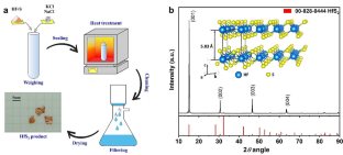
Layered two-dimensional materials are promising candidates for next-generation semiconductor platforms owing to their atomically thin bodies, and it is crucial to develop a method for their large-scale synthesis for integrating these materials into the fabrication process. Here, we report the synthesis of a centimeter-scale HfS2 ingot using the molten salt flux method (MSFM). The structure, crystallinity, and uniformity of the synthesized HfS2 sample were verified using X-ray diffraction and Raman spectroscopy. The chemical properties were investigated using X-ray photoelectron spectroscopy. A HfS2 synaptic field effect transistor (FET) was fabricated to confirm its electrical uniformity and semiconducting nature, with an average mobility of 10.6 cm2 V-1 s-1. The synaptic plasticity of the HfS2 synaptic FET was investigated by applying light pulses (405 nm) in different modulation configurations. Paired-pulse facilitation was achieved by applying a continuous light pulse with a negative gate bias voltage. The modulation of synaptic weight was demonstrated under different stimulation conditions, which emulates the human brain. Furthermore, the linearity of the HfS2 synaptic device was optimized based on the frequency of the pulses to enhance learning accuracy. The approach reported here encourages the large-scaled production of transition metal dichalcogenides (TMDs) for use in artificial synaptic transistors.
期刊介绍:
Electronic Materials Letters is an official journal of the Korean Institute of Metals and Materials. It is a peer-reviewed international journal publishing print and online version. It covers all disciplines of research and technology in electronic materials. Emphasis is placed on science, engineering and applications of advanced materials, including electronic, magnetic, optical, organic, electrochemical, mechanical, and nanoscale materials. The aspects of synthesis and processing include thin films, nanostructures, self assembly, and bulk, all related to thermodynamics, kinetics and/or modeling.


 分享
分享
 求助内容:
求助内容: 应助结果提醒方式:
 扫码关注我们
