{"title":"在 25-600 V 混合模式 SiC CMOS 技术中集成了栅极驱动器和低压控制器的 400 V 降压转换器","authors":"Utsav Gupta, Hua Zhang, Tianshi Liu, Sundar Isukapati, Emran Ashik, Adam Morgan, Bongmook Lee, Woongje Sung, Anant Agarwal, Ayman Fayed","doi":"10.1007/s10470-024-02270-3","DOIUrl":null,"url":null,"abstract":"<div><p>This paper offers the first demonstration of the design and layout of a fully integrated power converter in a monolithic Silicon Carbide (SiC) technology. A 400 V Buck Converter integrated with Gate-Drivers and Low-Voltage Control circuitry in a 25–600 V Mixed-Mode SiC CMOS technology has been presented in this paper. A new SiC technology has been developed for this design which has a feature size of 1 μm. This technology allows integration of High-Voltage Power FETs and Low-Voltage CMOS circuits on the same die with a common substrate. Both high-side and low-side Power FETs are N-type hence a bootstrap circuit is used, and the gate drivers use an isolated capacitive level shifter to translate the signals from the 25 V domain to the 400 V domain which is the input voltage of the Buck Converter. The load current is 1 A and the nominal output voltage is 100 V thereby meaning that the output power is 100 W. The switching frequency is up to 1 MHz, and the duty cycle can range from 10% to 90% signifying a wide range of operation of the converter.</p></div>","PeriodicalId":7827,"journal":{"name":"Analog Integrated Circuits and Signal Processing","volume":"119 3","pages":"463 - 474"},"PeriodicalIF":1.4000,"publicationDate":"2024-04-23","publicationTypes":"Journal Article","fieldsOfStudy":null,"isOpenAccess":false,"openAccessPdf":"","citationCount":"0","resultStr":"{\"title\":\"A 400 V Buck Converter integrated with Gate-Drivers and low-voltage Controller in a 25–600 V mixed-mode SiC CMOS technology\",\"authors\":\"Utsav Gupta, Hua Zhang, Tianshi Liu, Sundar Isukapati, Emran Ashik, Adam Morgan, Bongmook Lee, Woongje Sung, Anant Agarwal, Ayman Fayed\",\"doi\":\"10.1007/s10470-024-02270-3\",\"DOIUrl\":null,\"url\":null,\"abstract\":\"<div><p>This paper offers the first demonstration of the design and layout of a fully integrated power converter in a monolithic Silicon Carbide (SiC) technology. A 400 V Buck Converter integrated with Gate-Drivers and Low-Voltage Control circuitry in a 25–600 V Mixed-Mode SiC CMOS technology has been presented in this paper. A new SiC technology has been developed for this design which has a feature size of 1 μm. This technology allows integration of High-Voltage Power FETs and Low-Voltage CMOS circuits on the same die with a common substrate. Both high-side and low-side Power FETs are N-type hence a bootstrap circuit is used, and the gate drivers use an isolated capacitive level shifter to translate the signals from the 25 V domain to the 400 V domain which is the input voltage of the Buck Converter. The load current is 1 A and the nominal output voltage is 100 V thereby meaning that the output power is 100 W. The switching frequency is up to 1 MHz, and the duty cycle can range from 10% to 90% signifying a wide range of operation of the converter.</p></div>\",\"PeriodicalId\":7827,\"journal\":{\"name\":\"Analog Integrated Circuits and Signal Processing\",\"volume\":\"119 3\",\"pages\":\"463 - 474\"},\"PeriodicalIF\":1.4000,\"publicationDate\":\"2024-04-23\",\"publicationTypes\":\"Journal Article\",\"fieldsOfStudy\":null,\"isOpenAccess\":false,\"openAccessPdf\":\"\",\"citationCount\":\"0\",\"resultStr\":null,\"platform\":\"Semanticscholar\",\"paperid\":null,\"PeriodicalName\":\"Analog Integrated Circuits and Signal Processing\",\"FirstCategoryId\":\"5\",\"ListUrlMain\":\"https://link.springer.com/article/10.1007/s10470-024-02270-3\",\"RegionNum\":4,\"RegionCategory\":\"工程技术\",\"ArticlePicture\":[],\"TitleCN\":null,\"AbstractTextCN\":null,\"PMCID\":null,\"EPubDate\":\"\",\"PubModel\":\"\",\"JCR\":\"Q4\",\"JCRName\":\"COMPUTER SCIENCE, HARDWARE & ARCHITECTURE\",\"Score\":null,\"Total\":0}","platform":"Semanticscholar","paperid":null,"PeriodicalName":"Analog Integrated Circuits and Signal Processing","FirstCategoryId":"5","ListUrlMain":"https://link.springer.com/article/10.1007/s10470-024-02270-3","RegionNum":4,"RegionCategory":"工程技术","ArticlePicture":[],"TitleCN":null,"AbstractTextCN":null,"PMCID":null,"EPubDate":"","PubModel":"","JCR":"Q4","JCRName":"COMPUTER SCIENCE, HARDWARE & ARCHITECTURE","Score":null,"Total":0}
引用次数: 0
摘要
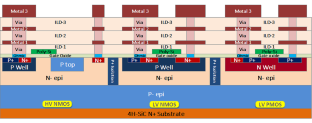
本文首次展示了采用单片碳化硅(SiC)技术的全集成功率转换器的设计和布局。本文介绍了在 25-600 V 混合模式 SiC CMOS 技术中集成了栅极驱动器和低压控制电路的 400 V 降压转换器。该设计采用了一种新的 SiC 技术,其特征尺寸为 1 μm。利用这种技术,可以在同一芯片上集成高压功率场效应晶体管和低压 CMOS 电路。高压侧和低压侧功率场效应晶体管均为 N 型,因此使用了自举电路,栅极驱动器使用隔离电容式电平转换器将信号从 25 V 域转换到 400 V 域,即降压转换器的输入电压。负载电流为 1 A,额定输出电压为 100 V,这意味着输出功率为 100 W。开关频率高达 1 MHz,占空比范围为 10% 至 90%,这意味着转换器的工作范围很广。
A 400 V Buck Converter integrated with Gate-Drivers and low-voltage Controller in a 25–600 V mixed-mode SiC CMOS technology
This paper offers the first demonstration of the design and layout of a fully integrated power converter in a monolithic Silicon Carbide (SiC) technology. A 400 V Buck Converter integrated with Gate-Drivers and Low-Voltage Control circuitry in a 25–600 V Mixed-Mode SiC CMOS technology has been presented in this paper. A new SiC technology has been developed for this design which has a feature size of 1 μm. This technology allows integration of High-Voltage Power FETs and Low-Voltage CMOS circuits on the same die with a common substrate. Both high-side and low-side Power FETs are N-type hence a bootstrap circuit is used, and the gate drivers use an isolated capacitive level shifter to translate the signals from the 25 V domain to the 400 V domain which is the input voltage of the Buck Converter. The load current is 1 A and the nominal output voltage is 100 V thereby meaning that the output power is 100 W. The switching frequency is up to 1 MHz, and the duty cycle can range from 10% to 90% signifying a wide range of operation of the converter.
期刊介绍:
Analog Integrated Circuits and Signal Processing is an archival peer reviewed journal dedicated to the design and application of analog, radio frequency (RF), and mixed signal integrated circuits (ICs) as well as signal processing circuits and systems. It features both new research results and tutorial views and reflects the large volume of cutting-edge research activity in the worldwide field today.
A partial list of topics includes analog and mixed signal interface circuits and systems; analog and RFIC design; data converters; active-RC, switched-capacitor, and continuous-time integrated filters; mixed analog/digital VLSI systems; wireless radio transceivers; clock and data recovery circuits; and high speed optoelectronic circuits and systems.


 分享
分享
 求助内容:
求助内容: 应助结果提醒方式:
 扫码关注我们
