Zaoyang Lin*, Xiangyu Wu, Daire Cott, Yuanyuan Shi, Henry Medina Silva, Stefanie Sergeant, Thierry Conard, Johan Meersschaut, Ankit Nalin Mehta, Benjamin Groven, Pierre Morin, Inge Asselberghs, Cesar Javier Lockhart de la Rosa, Gouri Sankar Kar, Dennis Lin* and Annelies Delabie*,
{"title":"基于二维过渡金属二卤化物的场效应晶体管的顶栅叠层工程,采用高κ铝酸钆界面层","authors":"Zaoyang Lin*, Xiangyu Wu, Daire Cott, Yuanyuan Shi, Henry Medina Silva, Stefanie Sergeant, Thierry Conard, Johan Meersschaut, Ankit Nalin Mehta, Benjamin Groven, Pierre Morin, Inge Asselberghs, Cesar Javier Lockhart de la Rosa, Gouri Sankar Kar, Dennis Lin* and Annelies Delabie*, ","doi":"10.1021/acsaelm.4c00309","DOIUrl":null,"url":null,"abstract":"<p >Atomic layer deposition (ALD) of gate dielectrics on two-dimensional transition-metal dichalcogenides (2D TMDs) is challenging due to their chemically inert surfaces. Although various surface pretreatments can form nucleation sites to facilitate the precursor adsorption, preserving 2D TMDs during the pretreatments and maintaining gate stack quality with the weak 2D TMD/dielectric interface become the main concerns. In this work, we combine physisorbed-precursor-assisted (PPA)-ALD to minimize damage to 2D TMDs with a second interfacial layer for performance enhancement. Ultrathin GdAlO<sub>3</sub> interlayers are integrated into 2D TMD gate stacks with PPA-ALD AlO<sub><i>x</i></sub> seeding layers and HfO<sub>2</sub> top dielectrics. Further, 1-nm-thick and pinhole-free GdAlO<sub>3</sub> can be deposited on AlO<sub><i>x</i></sub>-seeded monolayer (1L) WS<sub>2</sub> by ALD at 250 °C. The material properties of 1L WS<sub>2</sub> are preserved, as confirmed by Raman spectroscopy. After the GdAlO<sub>3</sub> layer insertion, 1L MoS<sub>2</sub> dual-gate (DG) field-effect transistors (FETs) show improved subthreshold swing (SS), field-effect mobility, and <i>I</i><sub>d</sub>–<i>V</i><sub>g</sub> hysteresis without compromising the capacitance-equivalent thickness (CET). The proposed strategy is wafer-scale compatible and extendable to the future nanosheet gate-all-around structures.</p>","PeriodicalId":3,"journal":{"name":"ACS Applied Electronic Materials","volume":"6 6","pages":"4213–4222"},"PeriodicalIF":4.7000,"publicationDate":"2024-05-23","publicationTypes":"Journal Article","fieldsOfStudy":null,"isOpenAccess":false,"openAccessPdf":"","citationCount":"0","resultStr":"{\"title\":\"Top-Gate Stack Engineering Featuring a High-κ Gadolinium Aluminate Interfacial Layer for Field-Effect Transistors Based on Two-Dimensional Transition-Metal Dichalcogenides\",\"authors\":\"Zaoyang Lin*, Xiangyu Wu, Daire Cott, Yuanyuan Shi, Henry Medina Silva, Stefanie Sergeant, Thierry Conard, Johan Meersschaut, Ankit Nalin Mehta, Benjamin Groven, Pierre Morin, Inge Asselberghs, Cesar Javier Lockhart de la Rosa, Gouri Sankar Kar, Dennis Lin* and Annelies Delabie*, \",\"doi\":\"10.1021/acsaelm.4c00309\",\"DOIUrl\":null,\"url\":null,\"abstract\":\"<p >Atomic layer deposition (ALD) of gate dielectrics on two-dimensional transition-metal dichalcogenides (2D TMDs) is challenging due to their chemically inert surfaces. Although various surface pretreatments can form nucleation sites to facilitate the precursor adsorption, preserving 2D TMDs during the pretreatments and maintaining gate stack quality with the weak 2D TMD/dielectric interface become the main concerns. In this work, we combine physisorbed-precursor-assisted (PPA)-ALD to minimize damage to 2D TMDs with a second interfacial layer for performance enhancement. Ultrathin GdAlO<sub>3</sub> interlayers are integrated into 2D TMD gate stacks with PPA-ALD AlO<sub><i>x</i></sub> seeding layers and HfO<sub>2</sub> top dielectrics. Further, 1-nm-thick and pinhole-free GdAlO<sub>3</sub> can be deposited on AlO<sub><i>x</i></sub>-seeded monolayer (1L) WS<sub>2</sub> by ALD at 250 °C. The material properties of 1L WS<sub>2</sub> are preserved, as confirmed by Raman spectroscopy. After the GdAlO<sub>3</sub> layer insertion, 1L MoS<sub>2</sub> dual-gate (DG) field-effect transistors (FETs) show improved subthreshold swing (SS), field-effect mobility, and <i>I</i><sub>d</sub>–<i>V</i><sub>g</sub> hysteresis without compromising the capacitance-equivalent thickness (CET). The proposed strategy is wafer-scale compatible and extendable to the future nanosheet gate-all-around structures.</p>\",\"PeriodicalId\":3,\"journal\":{\"name\":\"ACS Applied Electronic Materials\",\"volume\":\"6 6\",\"pages\":\"4213–4222\"},\"PeriodicalIF\":4.7000,\"publicationDate\":\"2024-05-23\",\"publicationTypes\":\"Journal Article\",\"fieldsOfStudy\":null,\"isOpenAccess\":false,\"openAccessPdf\":\"\",\"citationCount\":\"0\",\"resultStr\":null,\"platform\":\"Semanticscholar\",\"paperid\":null,\"PeriodicalName\":\"ACS Applied Electronic Materials\",\"FirstCategoryId\":\"88\",\"ListUrlMain\":\"https://pubs.acs.org/doi/10.1021/acsaelm.4c00309\",\"RegionNum\":3,\"RegionCategory\":\"材料科学\",\"ArticlePicture\":[],\"TitleCN\":null,\"AbstractTextCN\":null,\"PMCID\":null,\"EPubDate\":\"\",\"PubModel\":\"\",\"JCR\":\"Q1\",\"JCRName\":\"ENGINEERING, ELECTRICAL & ELECTRONIC\",\"Score\":null,\"Total\":0}","platform":"Semanticscholar","paperid":null,"PeriodicalName":"ACS Applied Electronic Materials","FirstCategoryId":"88","ListUrlMain":"https://pubs.acs.org/doi/10.1021/acsaelm.4c00309","RegionNum":3,"RegionCategory":"材料科学","ArticlePicture":[],"TitleCN":null,"AbstractTextCN":null,"PMCID":null,"EPubDate":"","PubModel":"","JCR":"Q1","JCRName":"ENGINEERING, ELECTRICAL & ELECTRONIC","Score":null,"Total":0}
Top-Gate Stack Engineering Featuring a High-κ Gadolinium Aluminate Interfacial Layer for Field-Effect Transistors Based on Two-Dimensional Transition-Metal Dichalcogenides
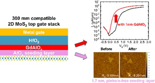
Atomic layer deposition (ALD) of gate dielectrics on two-dimensional transition-metal dichalcogenides (2D TMDs) is challenging due to their chemically inert surfaces. Although various surface pretreatments can form nucleation sites to facilitate the precursor adsorption, preserving 2D TMDs during the pretreatments and maintaining gate stack quality with the weak 2D TMD/dielectric interface become the main concerns. In this work, we combine physisorbed-precursor-assisted (PPA)-ALD to minimize damage to 2D TMDs with a second interfacial layer for performance enhancement. Ultrathin GdAlO3 interlayers are integrated into 2D TMD gate stacks with PPA-ALD AlOx seeding layers and HfO2 top dielectrics. Further, 1-nm-thick and pinhole-free GdAlO3 can be deposited on AlOx-seeded monolayer (1L) WS2 by ALD at 250 °C. The material properties of 1L WS2 are preserved, as confirmed by Raman spectroscopy. After the GdAlO3 layer insertion, 1L MoS2 dual-gate (DG) field-effect transistors (FETs) show improved subthreshold swing (SS), field-effect mobility, and Id–Vg hysteresis without compromising the capacitance-equivalent thickness (CET). The proposed strategy is wafer-scale compatible and extendable to the future nanosheet gate-all-around structures.
期刊介绍:
ACS Applied Electronic Materials is an interdisciplinary journal publishing original research covering all aspects of electronic materials. The journal is devoted to reports of new and original experimental and theoretical research of an applied nature that integrate knowledge in the areas of materials science, engineering, optics, physics, and chemistry into important applications of electronic materials. Sample research topics that span the journal's scope are inorganic, organic, ionic and polymeric materials with properties that include conducting, semiconducting, superconducting, insulating, dielectric, magnetic, optoelectronic, piezoelectric, ferroelectric and thermoelectric.
Indexed/Abstracted:
Web of Science SCIE
Scopus
CAS
INSPEC
Portico


 分享
分享
 求助内容:
求助内容: 应助结果提醒方式:
 扫码关注我们
