{"title":"Cu6GeWS8:具有直接带隙和超低晶格导热性的二维季硫化物","authors":"Yu-Tong Feng, Ying Zhu, Jiafu Wang, Jun-Hui Yuan","doi":"10.1007/s11664-024-11159-w","DOIUrl":null,"url":null,"abstract":"<div><p>Two-dimensional (2D) semiconductors are widely regarded as promising contenders for the next generation of optoelectronics and microelectronics, rendering the development of novel 2D semiconductors a focal point in current research. In this study, our attention is directed towards the non-van der Waals material Cu<sub>6</sub>GeWS<sub>8</sub>, where we have successfully predicted a stable 2D monolayer, designated as 2D Cu<sub>6</sub>GeWS<sub>8</sub>. This monolayer exhibits a direct bandgap of 1.709 eV, which maintains its robustness under biaxial strain ranging from −4% to 3%. Remarkably, the monolayer Cu<sub>6</sub>GeWS<sub>8</sub> showcases high hole mobility and demonstrates a moderate optical absorption coefficient across the visible and ultraviolet spectra. Notably, our investigation reveals that the monolayer Cu<sub>6</sub>GeWS<sub>8</sub> possesses an exceptionally low lattice thermal conductivity of 0.593 W m<sup>−1</sup> K<sup>−1</sup> at room temperature. These findings underscore the excellent physical characteristics of the predicted monolayer Cu<sub>6</sub>GeWS<sub>8</sub>, positioning it as a promising candidate for advanced low-dimensional devices.</p></div>","PeriodicalId":626,"journal":{"name":"Journal of Electronic Materials","volume":"53 7","pages":"3822 - 3833"},"PeriodicalIF":2.8000,"publicationDate":"2024-05-22","publicationTypes":"Journal Article","fieldsOfStudy":null,"isOpenAccess":false,"openAccessPdf":"","citationCount":"0","resultStr":"{\"title\":\"Cu6GeWS8: A Two-Dimensional Quaternary Sulfide with Direct Bandgap and Ultralow Lattice Thermal Conductivity\",\"authors\":\"Yu-Tong Feng, Ying Zhu, Jiafu Wang, Jun-Hui Yuan\",\"doi\":\"10.1007/s11664-024-11159-w\",\"DOIUrl\":null,\"url\":null,\"abstract\":\"<div><p>Two-dimensional (2D) semiconductors are widely regarded as promising contenders for the next generation of optoelectronics and microelectronics, rendering the development of novel 2D semiconductors a focal point in current research. In this study, our attention is directed towards the non-van der Waals material Cu<sub>6</sub>GeWS<sub>8</sub>, where we have successfully predicted a stable 2D monolayer, designated as 2D Cu<sub>6</sub>GeWS<sub>8</sub>. This monolayer exhibits a direct bandgap of 1.709 eV, which maintains its robustness under biaxial strain ranging from −4% to 3%. Remarkably, the monolayer Cu<sub>6</sub>GeWS<sub>8</sub> showcases high hole mobility and demonstrates a moderate optical absorption coefficient across the visible and ultraviolet spectra. Notably, our investigation reveals that the monolayer Cu<sub>6</sub>GeWS<sub>8</sub> possesses an exceptionally low lattice thermal conductivity of 0.593 W m<sup>−1</sup> K<sup>−1</sup> at room temperature. These findings underscore the excellent physical characteristics of the predicted monolayer Cu<sub>6</sub>GeWS<sub>8</sub>, positioning it as a promising candidate for advanced low-dimensional devices.</p></div>\",\"PeriodicalId\":626,\"journal\":{\"name\":\"Journal of Electronic Materials\",\"volume\":\"53 7\",\"pages\":\"3822 - 3833\"},\"PeriodicalIF\":2.8000,\"publicationDate\":\"2024-05-22\",\"publicationTypes\":\"Journal Article\",\"fieldsOfStudy\":null,\"isOpenAccess\":false,\"openAccessPdf\":\"\",\"citationCount\":\"0\",\"resultStr\":null,\"platform\":\"Semanticscholar\",\"paperid\":null,\"PeriodicalName\":\"Journal of Electronic Materials\",\"FirstCategoryId\":\"5\",\"ListUrlMain\":\"https://link.springer.com/article/10.1007/s11664-024-11159-w\",\"RegionNum\":4,\"RegionCategory\":\"工程技术\",\"ArticlePicture\":[],\"TitleCN\":null,\"AbstractTextCN\":null,\"PMCID\":null,\"EPubDate\":\"\",\"PubModel\":\"\",\"JCR\":\"Q3\",\"JCRName\":\"ENGINEERING, ELECTRICAL & ELECTRONIC\",\"Score\":null,\"Total\":0}","platform":"Semanticscholar","paperid":null,"PeriodicalName":"Journal of Electronic Materials","FirstCategoryId":"5","ListUrlMain":"https://link.springer.com/article/10.1007/s11664-024-11159-w","RegionNum":4,"RegionCategory":"工程技术","ArticlePicture":[],"TitleCN":null,"AbstractTextCN":null,"PMCID":null,"EPubDate":"","PubModel":"","JCR":"Q3","JCRName":"ENGINEERING, ELECTRICAL & ELECTRONIC","Score":null,"Total":0}
引用次数: 0
摘要
二维(2D)半导体被广泛认为是下一代光电子和微电子的有前途的竞争者,使得新型二维半导体的发展成为当前研究的焦点。在这项研究中,我们的注意力集中在非范德华材料Cu6GeWS8上,我们已经成功地预测了一个稳定的二维单层,命名为2D Cu6GeWS8。该单层膜的直接带隙为1.709 eV,在- 4% ~ 3%的双轴应变范围内保持其鲁棒性。值得注意的是,单层Cu6GeWS8显示出高空穴迁移率,并在可见和紫外光谱中表现出适度的光学吸收系数。值得注意的是,我们的研究表明,单层Cu6GeWS8在室温下具有非常低的晶格导热系数,为0.593 W m−1 K−1。这些发现强调了所预测的单层Cu6GeWS8的优异物理特性,使其成为先进低维器件的有前途的候选者。
Cu6GeWS8: A Two-Dimensional Quaternary Sulfide with Direct Bandgap and Ultralow Lattice Thermal Conductivity
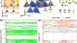
Two-dimensional (2D) semiconductors are widely regarded as promising contenders for the next generation of optoelectronics and microelectronics, rendering the development of novel 2D semiconductors a focal point in current research. In this study, our attention is directed towards the non-van der Waals material Cu6GeWS8, where we have successfully predicted a stable 2D monolayer, designated as 2D Cu6GeWS8. This monolayer exhibits a direct bandgap of 1.709 eV, which maintains its robustness under biaxial strain ranging from −4% to 3%. Remarkably, the monolayer Cu6GeWS8 showcases high hole mobility and demonstrates a moderate optical absorption coefficient across the visible and ultraviolet spectra. Notably, our investigation reveals that the monolayer Cu6GeWS8 possesses an exceptionally low lattice thermal conductivity of 0.593 W m−1 K−1 at room temperature. These findings underscore the excellent physical characteristics of the predicted monolayer Cu6GeWS8, positioning it as a promising candidate for advanced low-dimensional devices.
期刊介绍:
The Journal of Electronic Materials (JEM) reports monthly on the science and technology of electronic materials, while examining new applications for semiconductors, magnetic alloys, dielectrics, nanoscale materials, and photonic materials. The journal welcomes articles on methods for preparing and evaluating the chemical, physical, electronic, and optical properties of these materials. Specific areas of interest are materials for state-of-the-art transistors, nanotechnology, electronic packaging, detectors, emitters, metallization, superconductivity, and energy applications.
Review papers on current topics enable individuals in the field of electronics to keep abreast of activities in areas peripheral to their own. JEM also selects papers from conferences such as the Electronic Materials Conference, the U.S. Workshop on the Physics and Chemistry of II-VI Materials, and the International Conference on Thermoelectrics. It benefits both specialists and non-specialists in the electronic materials field.
A journal of The Minerals, Metals & Materials Society.




 京公网安备 11010802042870号
京ICP备2023020795号-1
京公网安备 11010802042870号
京ICP备2023020795号-1

 分享
分享
 求助内容:
求助内容: 应助结果提醒方式:
 扫码关注我们
