Kwang Jae Lee, Yeong Jae Kim, Jung-Hong Min, Chun Hong Kang, Ram Chandra Subedi, Huafan Zhang, Latifah Al-Maghrabi, Kwangwook Park, Dante Ahn, Yusin Pak, Tien Khee Ng, Young Min Song, Boon S. Ooi, Osman M. Bakr, Jungwook Min
{"title":"堆叠在玻璃氮化镓纳米线上的 MAPbI3 的特性","authors":"Kwang Jae Lee, Yeong Jae Kim, Jung-Hong Min, Chun Hong Kang, Ram Chandra Subedi, Huafan Zhang, Latifah Al-Maghrabi, Kwangwook Park, Dante Ahn, Yusin Pak, Tien Khee Ng, Young Min Song, Boon S. Ooi, Osman M. Bakr, Jungwook Min","doi":"10.1002/aelm.202400095","DOIUrl":null,"url":null,"abstract":"<p>When implementing optoelectronic devices through the stacking of heterogeneous materials, considering the bandgap offset is crucial for achieving efficient carrier dynamics. In this study, the bandgap offset characteristics are investigated when <i>n</i>-type gallium nitride nanowires (<i>n</i>-GaN NWs) are used as electron transport layers in methylammonium lead iodide (MAPbI<sub>3</sub>)-based optoelectronic devices. <i>n</i>-GaN NWs are grown on indium-tin-oxide (ITO)-coated glass via the plasma-assisted molecular beam epitaxy (PA-MBE) process to form the “GaN NWs-on-glass” platform. A MAPbI<sub>3</sub> thin film is then spin-coated on the GaN NWs-on-glass. X-ray photoelectron spectroscopy (XPS) shows that the valence and conduction band offsets in the MAPbI<sub>3</sub>/<i>n</i>-GaN heterostructure are 2.19 and 0.40 eV, respectively, indicating a type-II band alignment ideal for optoelectronic applications. Prototype photovoltaic devices stacking perovskite on GaN NWs-on-glass show excellent interfacial charge-transfer ability, photon recycling, and carrier extraction efficiency. As a pioneering step in exploiting the diverse potential of the GaN-on-glass, it is demonstrated that the junction characteristics of MAPbI<sub>3</sub>/<i>n</i>-GaN NW heterostructures can lead to a variety of optoelectronic device applications.</p>","PeriodicalId":110,"journal":{"name":"Advanced Electronic Materials","volume":"10 10","pages":""},"PeriodicalIF":5.3000,"publicationDate":"2024-05-30","publicationTypes":"Journal Article","fieldsOfStudy":null,"isOpenAccess":false,"openAccessPdf":"https://onlinelibrary.wiley.com/doi/epdf/10.1002/aelm.202400095","citationCount":"0","resultStr":"{\"title\":\"Characteristics of MAPbI3 Stacked on the GaN Nanowires-On-Glass\",\"authors\":\"Kwang Jae Lee, Yeong Jae Kim, Jung-Hong Min, Chun Hong Kang, Ram Chandra Subedi, Huafan Zhang, Latifah Al-Maghrabi, Kwangwook Park, Dante Ahn, Yusin Pak, Tien Khee Ng, Young Min Song, Boon S. Ooi, Osman M. Bakr, Jungwook Min\",\"doi\":\"10.1002/aelm.202400095\",\"DOIUrl\":null,\"url\":null,\"abstract\":\"<p>When implementing optoelectronic devices through the stacking of heterogeneous materials, considering the bandgap offset is crucial for achieving efficient carrier dynamics. In this study, the bandgap offset characteristics are investigated when <i>n</i>-type gallium nitride nanowires (<i>n</i>-GaN NWs) are used as electron transport layers in methylammonium lead iodide (MAPbI<sub>3</sub>)-based optoelectronic devices. <i>n</i>-GaN NWs are grown on indium-tin-oxide (ITO)-coated glass via the plasma-assisted molecular beam epitaxy (PA-MBE) process to form the “GaN NWs-on-glass” platform. A MAPbI<sub>3</sub> thin film is then spin-coated on the GaN NWs-on-glass. X-ray photoelectron spectroscopy (XPS) shows that the valence and conduction band offsets in the MAPbI<sub>3</sub>/<i>n</i>-GaN heterostructure are 2.19 and 0.40 eV, respectively, indicating a type-II band alignment ideal for optoelectronic applications. Prototype photovoltaic devices stacking perovskite on GaN NWs-on-glass show excellent interfacial charge-transfer ability, photon recycling, and carrier extraction efficiency. As a pioneering step in exploiting the diverse potential of the GaN-on-glass, it is demonstrated that the junction characteristics of MAPbI<sub>3</sub>/<i>n</i>-GaN NW heterostructures can lead to a variety of optoelectronic device applications.</p>\",\"PeriodicalId\":110,\"journal\":{\"name\":\"Advanced Electronic Materials\",\"volume\":\"10 10\",\"pages\":\"\"},\"PeriodicalIF\":5.3000,\"publicationDate\":\"2024-05-30\",\"publicationTypes\":\"Journal Article\",\"fieldsOfStudy\":null,\"isOpenAccess\":false,\"openAccessPdf\":\"https://onlinelibrary.wiley.com/doi/epdf/10.1002/aelm.202400095\",\"citationCount\":\"0\",\"resultStr\":null,\"platform\":\"Semanticscholar\",\"paperid\":null,\"PeriodicalName\":\"Advanced Electronic Materials\",\"FirstCategoryId\":\"88\",\"ListUrlMain\":\"https://advanced.onlinelibrary.wiley.com/doi/10.1002/aelm.202400095\",\"RegionNum\":2,\"RegionCategory\":\"材料科学\",\"ArticlePicture\":[],\"TitleCN\":null,\"AbstractTextCN\":null,\"PMCID\":null,\"EPubDate\":\"\",\"PubModel\":\"\",\"JCR\":\"Q2\",\"JCRName\":\"MATERIALS SCIENCE, MULTIDISCIPLINARY\",\"Score\":null,\"Total\":0}","platform":"Semanticscholar","paperid":null,"PeriodicalName":"Advanced Electronic Materials","FirstCategoryId":"88","ListUrlMain":"https://advanced.onlinelibrary.wiley.com/doi/10.1002/aelm.202400095","RegionNum":2,"RegionCategory":"材料科学","ArticlePicture":[],"TitleCN":null,"AbstractTextCN":null,"PMCID":null,"EPubDate":"","PubModel":"","JCR":"Q2","JCRName":"MATERIALS SCIENCE, MULTIDISCIPLINARY","Score":null,"Total":0}
引用次数: 0
摘要
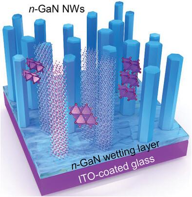
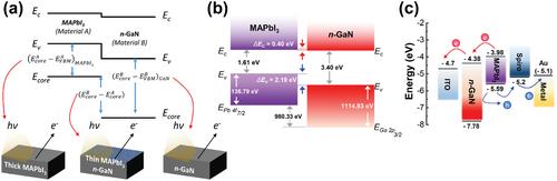
在通过堆叠异质材料实现光电器件时,考虑带隙偏移对于实现高效载流子动力学至关重要。本研究通过等离子体辅助分子束外延(PA-MBE)工艺,将 n 型氮化镓纳米线(n-GaN NWs)生长在涂有铟锡氧化物(ITO)的玻璃上,形成 "GaN NWs-on-glass "平台。然后在玻璃上的氮化镓氮瓦上旋涂 MAPbI3 薄膜。X 射线光电子能谱(XPS)显示,MAPbI3/n-GaN 异质结构中的价带和导带偏移分别为 2.19 和 0.40 eV,这表明其 II 型带排列非常适合光电应用。在玻璃基氮化镓氮瓦上堆叠过氧化物的光伏器件原型显示出卓越的界面电荷转移能力、光子回收和载流子萃取效率。作为开发玻璃基氮化镓各种潜能的先驱,研究表明 MAPbI3/n-GaN NW 异质结构的结特性可带来各种光电器件应用。
Characteristics of MAPbI3 Stacked on the GaN Nanowires-On-Glass
When implementing optoelectronic devices through the stacking of heterogeneous materials, considering the bandgap offset is crucial for achieving efficient carrier dynamics. In this study, the bandgap offset characteristics are investigated when n-type gallium nitride nanowires (n-GaN NWs) are used as electron transport layers in methylammonium lead iodide (MAPbI3)-based optoelectronic devices. n-GaN NWs are grown on indium-tin-oxide (ITO)-coated glass via the plasma-assisted molecular beam epitaxy (PA-MBE) process to form the “GaN NWs-on-glass” platform. A MAPbI3 thin film is then spin-coated on the GaN NWs-on-glass. X-ray photoelectron spectroscopy (XPS) shows that the valence and conduction band offsets in the MAPbI3/n-GaN heterostructure are 2.19 and 0.40 eV, respectively, indicating a type-II band alignment ideal for optoelectronic applications. Prototype photovoltaic devices stacking perovskite on GaN NWs-on-glass show excellent interfacial charge-transfer ability, photon recycling, and carrier extraction efficiency. As a pioneering step in exploiting the diverse potential of the GaN-on-glass, it is demonstrated that the junction characteristics of MAPbI3/n-GaN NW heterostructures can lead to a variety of optoelectronic device applications.
期刊介绍:
Advanced Electronic Materials is an interdisciplinary forum for peer-reviewed, high-quality, high-impact research in the fields of materials science, physics, and engineering of electronic and magnetic materials. It includes research on physics and physical properties of electronic and magnetic materials, spintronics, electronics, device physics and engineering, micro- and nano-electromechanical systems, and organic electronics, in addition to fundamental research.


 分享
分享
 求助内容:
求助内容: 应助结果提醒方式:
 扫码关注我们
