Mingyuan Sheng, Xi Chang, Xiaojun Mao, Yang Gao, Xiaoyang Xuan, Haifen Xie, Haichuan Mu, Yueping Niu, Shangqing Gong, Min Qian
{"title":"WS2/MoSe2 侧向异质结构的生长与光响应","authors":"Mingyuan Sheng, Xi Chang, Xiaojun Mao, Yang Gao, Xiaoyang Xuan, Haifen Xie, Haichuan Mu, Yueping Niu, Shangqing Gong, Min Qian","doi":"10.1002/aelm.202300842","DOIUrl":null,"url":null,"abstract":"<p>The heterostructure of two-dimensional transition metal dichalcogenide (TMDC) has garnered extensive attention, for the junction is the building block of a semiconductor device. However, the controllable synthesis of TMDC heterostructures of different transition metals and different chalcogen elements is still challenging because of the etching by atom substitution during the chemical vapor deposition (CVD) process. Here, a Mo─O transition state with lower energy is introduced to the edge of an as-grown MoSe<sub>2</sub> by using ultraviolet ozone treatment, to prevent the fast atom substitution of S for Se, and enable a stable growth of WS<sub>2</sub>/MoSe<sub>2</sub> lateral heterostructure. A polymer-free transfer method is developed based on capillary interaction, and atomic structure characterization confirms the high-quality WS<sub>2</sub>/MoSe<sub>2</sub> lateral heterostructure. The WS<sub>2</sub>/MoSe<sub>2</sub> lateral heterostructure photodetector exhibits superior photoresponse compared to WS<sub>2</sub> and MoSe<sub>2</sub> devices, with a responsivity of 21.87 A W<sup>−1</sup> and a detectivity of 4.2 × 10<sup>12</sup> Jones at 350 nm. Kelvin probe force microscopy result reveals that the built-in electric field within the heterojunction facilitates the effective separation of photogenerated electron-hole pairs. This study carries profound implications for the CVD growth and polymer-free transfer of TMDC heterostructures in photodetector applications.</p>","PeriodicalId":110,"journal":{"name":"Advanced Electronic Materials","volume":"10 8","pages":""},"PeriodicalIF":5.3000,"publicationDate":"2024-05-30","publicationTypes":"Journal Article","fieldsOfStudy":null,"isOpenAccess":false,"openAccessPdf":"https://onlinelibrary.wiley.com/doi/epdf/10.1002/aelm.202300842","citationCount":"0","resultStr":"{\"title\":\"Growth and Photoresponse of WS2/MoSe2 Lateral Heterostructure\",\"authors\":\"Mingyuan Sheng, Xi Chang, Xiaojun Mao, Yang Gao, Xiaoyang Xuan, Haifen Xie, Haichuan Mu, Yueping Niu, Shangqing Gong, Min Qian\",\"doi\":\"10.1002/aelm.202300842\",\"DOIUrl\":null,\"url\":null,\"abstract\":\"<p>The heterostructure of two-dimensional transition metal dichalcogenide (TMDC) has garnered extensive attention, for the junction is the building block of a semiconductor device. However, the controllable synthesis of TMDC heterostructures of different transition metals and different chalcogen elements is still challenging because of the etching by atom substitution during the chemical vapor deposition (CVD) process. Here, a Mo─O transition state with lower energy is introduced to the edge of an as-grown MoSe<sub>2</sub> by using ultraviolet ozone treatment, to prevent the fast atom substitution of S for Se, and enable a stable growth of WS<sub>2</sub>/MoSe<sub>2</sub> lateral heterostructure. A polymer-free transfer method is developed based on capillary interaction, and atomic structure characterization confirms the high-quality WS<sub>2</sub>/MoSe<sub>2</sub> lateral heterostructure. The WS<sub>2</sub>/MoSe<sub>2</sub> lateral heterostructure photodetector exhibits superior photoresponse compared to WS<sub>2</sub> and MoSe<sub>2</sub> devices, with a responsivity of 21.87 A W<sup>−1</sup> and a detectivity of 4.2 × 10<sup>12</sup> Jones at 350 nm. Kelvin probe force microscopy result reveals that the built-in electric field within the heterojunction facilitates the effective separation of photogenerated electron-hole pairs. This study carries profound implications for the CVD growth and polymer-free transfer of TMDC heterostructures in photodetector applications.</p>\",\"PeriodicalId\":110,\"journal\":{\"name\":\"Advanced Electronic Materials\",\"volume\":\"10 8\",\"pages\":\"\"},\"PeriodicalIF\":5.3000,\"publicationDate\":\"2024-05-30\",\"publicationTypes\":\"Journal Article\",\"fieldsOfStudy\":null,\"isOpenAccess\":false,\"openAccessPdf\":\"https://onlinelibrary.wiley.com/doi/epdf/10.1002/aelm.202300842\",\"citationCount\":\"0\",\"resultStr\":null,\"platform\":\"Semanticscholar\",\"paperid\":null,\"PeriodicalName\":\"Advanced Electronic Materials\",\"FirstCategoryId\":\"88\",\"ListUrlMain\":\"https://advanced.onlinelibrary.wiley.com/doi/10.1002/aelm.202300842\",\"RegionNum\":2,\"RegionCategory\":\"材料科学\",\"ArticlePicture\":[],\"TitleCN\":null,\"AbstractTextCN\":null,\"PMCID\":null,\"EPubDate\":\"\",\"PubModel\":\"\",\"JCR\":\"Q2\",\"JCRName\":\"MATERIALS SCIENCE, MULTIDISCIPLINARY\",\"Score\":null,\"Total\":0}","platform":"Semanticscholar","paperid":null,"PeriodicalName":"Advanced Electronic Materials","FirstCategoryId":"88","ListUrlMain":"https://advanced.onlinelibrary.wiley.com/doi/10.1002/aelm.202300842","RegionNum":2,"RegionCategory":"材料科学","ArticlePicture":[],"TitleCN":null,"AbstractTextCN":null,"PMCID":null,"EPubDate":"","PubModel":"","JCR":"Q2","JCRName":"MATERIALS SCIENCE, MULTIDISCIPLINARY","Score":null,"Total":0}
Growth and Photoresponse of WS2/MoSe2 Lateral Heterostructure
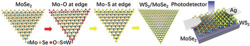
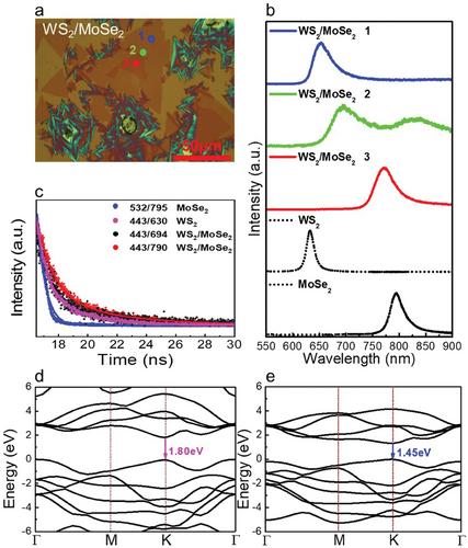
The heterostructure of two-dimensional transition metal dichalcogenide (TMDC) has garnered extensive attention, for the junction is the building block of a semiconductor device. However, the controllable synthesis of TMDC heterostructures of different transition metals and different chalcogen elements is still challenging because of the etching by atom substitution during the chemical vapor deposition (CVD) process. Here, a Mo─O transition state with lower energy is introduced to the edge of an as-grown MoSe2 by using ultraviolet ozone treatment, to prevent the fast atom substitution of S for Se, and enable a stable growth of WS2/MoSe2 lateral heterostructure. A polymer-free transfer method is developed based on capillary interaction, and atomic structure characterization confirms the high-quality WS2/MoSe2 lateral heterostructure. The WS2/MoSe2 lateral heterostructure photodetector exhibits superior photoresponse compared to WS2 and MoSe2 devices, with a responsivity of 21.87 A W−1 and a detectivity of 4.2 × 10¹² Jones at 350 nm. Kelvin probe force microscopy result reveals that the built-in electric field within the heterojunction facilitates the effective separation of photogenerated electron-hole pairs. This study carries profound implications for the CVD growth and polymer-free transfer of TMDC heterostructures in photodetector applications.
期刊介绍:
Advanced Electronic Materials is an interdisciplinary forum for peer-reviewed, high-quality, high-impact research in the fields of materials science, physics, and engineering of electronic and magnetic materials. It includes research on physics and physical properties of electronic and magnetic materials, spintronics, electronics, device physics and engineering, micro- and nano-electromechanical systems, and organic electronics, in addition to fundamental research.


 分享
分享
 求助内容:
求助内容: 应助结果提醒方式:
 扫码关注我们
