Yuwen Su, Yingtao Ding, Lei Xiao, Ziyue Zhang, Yangyang Yan, Zhifang Liu, Zhiming Chen, Huikai Xie
{"title":"通过基于双催化的无电解电镀组合阻挡层和种子层,实现超深 TSV 技术。","authors":"Yuwen Su, Yingtao Ding, Lei Xiao, Ziyue Zhang, Yangyang Yan, Zhifang Liu, Zhiming Chen, Huikai Xie","doi":"10.1038/s41378-024-00713-5","DOIUrl":null,"url":null,"abstract":"<p><p>Silicon interposers embedded with ultra-deep through-silicon vias (TSVs) are in great demand for the heterogeneous integration and packaging of opto-electronic chiplets and microelectromechanical systems (MEMS) devices. Considering the cost-effective and reliable manufacturing of ultra-deep TSVs, the formation of continuous barrier and seed layers remains a crucial challenge to solve. Herein, we present a novel dual catalysis-based electroless plating (ELP) technique by tailoring polyimide (PI) liner surfaces to fabricate dense combined Ni barrier/seed layers in ultra-deep TSVs. In additional to the conventional acid catalysis procedure, a prior catalytic step in an alkaline environment is proposed to hydrolyze the PI surface into a polyamide acid (PAA) interfacial layer, resulting in additional catalysts and the formation of a dense Ni layer that can function as both a barrier layer and a seed layer, particularly at the bottom of the deep TSV. TSVs with depths larger than 500 μm and no voids are successfully fabricated in this study. The fabrication process involves low costs and temperatures. For a fabricated 530-μm-deep TSV with a diameter of 70 μm, the measured depletion capacitance and leakage current are approximately 1.3 pF and 1.7 pA at 20 V, respectively, indicating good electrical properties. The proposed fabrication strategy can provide a cost-effective and feasible solution to the challenge of manufacturing ultra-deep TSVs for modern 3D heterogeneous integration and packaging applications.</p>","PeriodicalId":18560,"journal":{"name":"Microsystems & Nanoengineering","volume":"10 ","pages":"76"},"PeriodicalIF":9.9000,"publicationDate":"2024-06-11","publicationTypes":"Journal Article","fieldsOfStudy":null,"isOpenAccess":false,"openAccessPdf":"https://www.ncbi.nlm.nih.gov/pmc/articles/PMC11164994/pdf/","citationCount":"0","resultStr":"{\"title\":\"An ultra-deep TSV technique enabled by the dual catalysis-based electroless plating of combined barrier and seed layers.\",\"authors\":\"Yuwen Su, Yingtao Ding, Lei Xiao, Ziyue Zhang, Yangyang Yan, Zhifang Liu, Zhiming Chen, Huikai Xie\",\"doi\":\"10.1038/s41378-024-00713-5\",\"DOIUrl\":null,\"url\":null,\"abstract\":\"<p><p>Silicon interposers embedded with ultra-deep through-silicon vias (TSVs) are in great demand for the heterogeneous integration and packaging of opto-electronic chiplets and microelectromechanical systems (MEMS) devices. Considering the cost-effective and reliable manufacturing of ultra-deep TSVs, the formation of continuous barrier and seed layers remains a crucial challenge to solve. Herein, we present a novel dual catalysis-based electroless plating (ELP) technique by tailoring polyimide (PI) liner surfaces to fabricate dense combined Ni barrier/seed layers in ultra-deep TSVs. In additional to the conventional acid catalysis procedure, a prior catalytic step in an alkaline environment is proposed to hydrolyze the PI surface into a polyamide acid (PAA) interfacial layer, resulting in additional catalysts and the formation of a dense Ni layer that can function as both a barrier layer and a seed layer, particularly at the bottom of the deep TSV. TSVs with depths larger than 500 μm and no voids are successfully fabricated in this study. The fabrication process involves low costs and temperatures. For a fabricated 530-μm-deep TSV with a diameter of 70 μm, the measured depletion capacitance and leakage current are approximately 1.3 pF and 1.7 pA at 20 V, respectively, indicating good electrical properties. The proposed fabrication strategy can provide a cost-effective and feasible solution to the challenge of manufacturing ultra-deep TSVs for modern 3D heterogeneous integration and packaging applications.</p>\",\"PeriodicalId\":18560,\"journal\":{\"name\":\"Microsystems & Nanoengineering\",\"volume\":\"10 \",\"pages\":\"76\"},\"PeriodicalIF\":9.9000,\"publicationDate\":\"2024-06-11\",\"publicationTypes\":\"Journal Article\",\"fieldsOfStudy\":null,\"isOpenAccess\":false,\"openAccessPdf\":\"https://www.ncbi.nlm.nih.gov/pmc/articles/PMC11164994/pdf/\",\"citationCount\":\"0\",\"resultStr\":null,\"platform\":\"Semanticscholar\",\"paperid\":null,\"PeriodicalName\":\"Microsystems & Nanoengineering\",\"FirstCategoryId\":\"5\",\"ListUrlMain\":\"https://doi.org/10.1038/s41378-024-00713-5\",\"RegionNum\":1,\"RegionCategory\":\"工程技术\",\"ArticlePicture\":[],\"TitleCN\":null,\"AbstractTextCN\":null,\"PMCID\":null,\"EPubDate\":\"2024/1/1 0:00:00\",\"PubModel\":\"eCollection\",\"JCR\":\"Q1\",\"JCRName\":\"INSTRUMENTS & INSTRUMENTATION\",\"Score\":null,\"Total\":0}","platform":"Semanticscholar","paperid":null,"PeriodicalName":"Microsystems & Nanoengineering","FirstCategoryId":"5","ListUrlMain":"https://doi.org/10.1038/s41378-024-00713-5","RegionNum":1,"RegionCategory":"工程技术","ArticlePicture":[],"TitleCN":null,"AbstractTextCN":null,"PMCID":null,"EPubDate":"2024/1/1 0:00:00","PubModel":"eCollection","JCR":"Q1","JCRName":"INSTRUMENTS & INSTRUMENTATION","Score":null,"Total":0}
An ultra-deep TSV technique enabled by the dual catalysis-based electroless plating of combined barrier and seed layers.
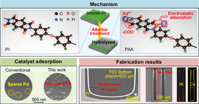
Silicon interposers embedded with ultra-deep through-silicon vias (TSVs) are in great demand for the heterogeneous integration and packaging of opto-electronic chiplets and microelectromechanical systems (MEMS) devices. Considering the cost-effective and reliable manufacturing of ultra-deep TSVs, the formation of continuous barrier and seed layers remains a crucial challenge to solve. Herein, we present a novel dual catalysis-based electroless plating (ELP) technique by tailoring polyimide (PI) liner surfaces to fabricate dense combined Ni barrier/seed layers in ultra-deep TSVs. In additional to the conventional acid catalysis procedure, a prior catalytic step in an alkaline environment is proposed to hydrolyze the PI surface into a polyamide acid (PAA) interfacial layer, resulting in additional catalysts and the formation of a dense Ni layer that can function as both a barrier layer and a seed layer, particularly at the bottom of the deep TSV. TSVs with depths larger than 500 μm and no voids are successfully fabricated in this study. The fabrication process involves low costs and temperatures. For a fabricated 530-μm-deep TSV with a diameter of 70 μm, the measured depletion capacitance and leakage current are approximately 1.3 pF and 1.7 pA at 20 V, respectively, indicating good electrical properties. The proposed fabrication strategy can provide a cost-effective and feasible solution to the challenge of manufacturing ultra-deep TSVs for modern 3D heterogeneous integration and packaging applications.
期刊介绍:
Microsystems & Nanoengineering is a comprehensive online journal that focuses on the field of Micro and Nano Electro Mechanical Systems (MEMS and NEMS). It provides a platform for researchers to share their original research findings and review articles in this area. The journal covers a wide range of topics, from fundamental research to practical applications. Published by Springer Nature, in collaboration with the Aerospace Information Research Institute, Chinese Academy of Sciences, and with the support of the State Key Laboratory of Transducer Technology, it is an esteemed publication in the field. As an open access journal, it offers free access to its content, allowing readers from around the world to benefit from the latest developments in MEMS and NEMS.


 分享
分享
 求助内容:
求助内容: 应助结果提醒方式:
 扫码关注我们
