Qihang Lv, Xia Shen, Xuyang Li, You Meng, Kin Man Yu, Pengfei Guo*, Liantuan Xiao*, Johnny C. Ho, Xidong Duan* and Xiangfeng Duan,
{"title":"用于高性能光电探测的轴向周期卤化物过氧化物超晶格的线上设计","authors":"Qihang Lv, Xia Shen, Xuyang Li, You Meng, Kin Man Yu, Pengfei Guo*, Liantuan Xiao*, Johnny C. Ho, Xidong Duan* and Xiangfeng Duan, ","doi":"10.1021/acsnano.4c05205","DOIUrl":null,"url":null,"abstract":"<p >Precise synthesis of all-inorganic lead halide perovskite nanowire heterostructures and superlattices with designable modulation of chemical compositions is essential for tailoring their optoelectronic properties. Nevertheless, controllable synthesis of perovskite nanostructure heterostructures remains challenging and underexplored to date. Here, we report a rational strategy for wafer-scale synthesis of one-dimensional periodic CsPbCl<sub>3</sub>/CsPbI<sub>3</sub> superlattices. We show that the highly parallel array of halide perovskite nanowires can be prepared roughly as horizontally guided growth on an <i>M</i>-plane sapphire. A periodic patterning of the sapphire substrate enables position-selective ion exchange to obtain highly periodic CsPbCl<sub>3</sub>/CsPbI<sub>3</sub> nanowire superlattices. This patterning is further confirmed by micro-photoluminescence investigations, which show that two separate band-edge emission peaks appear at the interface of a CsPbCl<sub>3</sub>/CsPbI<sub>3</sub> heterojunction. Additionally, compared with the pure CsPbCl<sub>3</sub> nanowires, photodetectors fabricated using these periodic heterostructure nanowires exhibit superior photoelectric performance, namely, high <i>I</i><sub>ON</sub>/<i>I</i><sub>OFF</sub> ratio (10<sup>4</sup>), higher responsivity (49 A/W), and higher detectivity (1.51 × 10<sup>13</sup> Jones). Moreover, a spatially resolved visible image sensor based on periodic nanowire superlattices is demonstrated with good imaging capability, suggesting promising application prospects in future photoelectronic imaging systems. All these results based on the periodic CsPbCl<sub>3</sub>/CsPbI<sub>3</sub> nanowire superlattices provides an attractive material platform for integrated perovskite devices and circuits.</p>","PeriodicalId":21,"journal":{"name":"ACS Nano","volume":"18 27","pages":"18022–18035"},"PeriodicalIF":16.0000,"publicationDate":"2024-06-27","publicationTypes":"Journal Article","fieldsOfStudy":null,"isOpenAccess":false,"openAccessPdf":"","citationCount":"0","resultStr":"{\"title\":\"On-Wire Design of Axial Periodic Halide Perovskite Superlattices for High-Performance Photodetection\",\"authors\":\"Qihang Lv, Xia Shen, Xuyang Li, You Meng, Kin Man Yu, Pengfei Guo*, Liantuan Xiao*, Johnny C. Ho, Xidong Duan* and Xiangfeng Duan, \",\"doi\":\"10.1021/acsnano.4c05205\",\"DOIUrl\":null,\"url\":null,\"abstract\":\"<p >Precise synthesis of all-inorganic lead halide perovskite nanowire heterostructures and superlattices with designable modulation of chemical compositions is essential for tailoring their optoelectronic properties. Nevertheless, controllable synthesis of perovskite nanostructure heterostructures remains challenging and underexplored to date. Here, we report a rational strategy for wafer-scale synthesis of one-dimensional periodic CsPbCl<sub>3</sub>/CsPbI<sub>3</sub> superlattices. We show that the highly parallel array of halide perovskite nanowires can be prepared roughly as horizontally guided growth on an <i>M</i>-plane sapphire. A periodic patterning of the sapphire substrate enables position-selective ion exchange to obtain highly periodic CsPbCl<sub>3</sub>/CsPbI<sub>3</sub> nanowire superlattices. This patterning is further confirmed by micro-photoluminescence investigations, which show that two separate band-edge emission peaks appear at the interface of a CsPbCl<sub>3</sub>/CsPbI<sub>3</sub> heterojunction. Additionally, compared with the pure CsPbCl<sub>3</sub> nanowires, photodetectors fabricated using these periodic heterostructure nanowires exhibit superior photoelectric performance, namely, high <i>I</i><sub>ON</sub>/<i>I</i><sub>OFF</sub> ratio (10<sup>4</sup>), higher responsivity (49 A/W), and higher detectivity (1.51 × 10<sup>13</sup> Jones). Moreover, a spatially resolved visible image sensor based on periodic nanowire superlattices is demonstrated with good imaging capability, suggesting promising application prospects in future photoelectronic imaging systems. All these results based on the periodic CsPbCl<sub>3</sub>/CsPbI<sub>3</sub> nanowire superlattices provides an attractive material platform for integrated perovskite devices and circuits.</p>\",\"PeriodicalId\":21,\"journal\":{\"name\":\"ACS Nano\",\"volume\":\"18 27\",\"pages\":\"18022–18035\"},\"PeriodicalIF\":16.0000,\"publicationDate\":\"2024-06-27\",\"publicationTypes\":\"Journal Article\",\"fieldsOfStudy\":null,\"isOpenAccess\":false,\"openAccessPdf\":\"\",\"citationCount\":\"0\",\"resultStr\":null,\"platform\":\"Semanticscholar\",\"paperid\":null,\"PeriodicalName\":\"ACS Nano\",\"FirstCategoryId\":\"88\",\"ListUrlMain\":\"https://pubs.acs.org/doi/10.1021/acsnano.4c05205\",\"RegionNum\":1,\"RegionCategory\":\"材料科学\",\"ArticlePicture\":[],\"TitleCN\":null,\"AbstractTextCN\":null,\"PMCID\":null,\"EPubDate\":\"\",\"PubModel\":\"\",\"JCR\":\"Q1\",\"JCRName\":\"CHEMISTRY, MULTIDISCIPLINARY\",\"Score\":null,\"Total\":0}","platform":"Semanticscholar","paperid":null,"PeriodicalName":"ACS Nano","FirstCategoryId":"88","ListUrlMain":"https://pubs.acs.org/doi/10.1021/acsnano.4c05205","RegionNum":1,"RegionCategory":"材料科学","ArticlePicture":[],"TitleCN":null,"AbstractTextCN":null,"PMCID":null,"EPubDate":"","PubModel":"","JCR":"Q1","JCRName":"CHEMISTRY, MULTIDISCIPLINARY","Score":null,"Total":0}
On-Wire Design of Axial Periodic Halide Perovskite Superlattices for High-Performance Photodetection
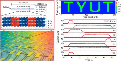
Precise synthesis of all-inorganic lead halide perovskite nanowire heterostructures and superlattices with designable modulation of chemical compositions is essential for tailoring their optoelectronic properties. Nevertheless, controllable synthesis of perovskite nanostructure heterostructures remains challenging and underexplored to date. Here, we report a rational strategy for wafer-scale synthesis of one-dimensional periodic CsPbCl3/CsPbI3 superlattices. We show that the highly parallel array of halide perovskite nanowires can be prepared roughly as horizontally guided growth on an M-plane sapphire. A periodic patterning of the sapphire substrate enables position-selective ion exchange to obtain highly periodic CsPbCl3/CsPbI3 nanowire superlattices. This patterning is further confirmed by micro-photoluminescence investigations, which show that two separate band-edge emission peaks appear at the interface of a CsPbCl3/CsPbI3 heterojunction. Additionally, compared with the pure CsPbCl3 nanowires, photodetectors fabricated using these periodic heterostructure nanowires exhibit superior photoelectric performance, namely, high ION/IOFF ratio (104), higher responsivity (49 A/W), and higher detectivity (1.51 × 10¹³ Jones). Moreover, a spatially resolved visible image sensor based on periodic nanowire superlattices is demonstrated with good imaging capability, suggesting promising application prospects in future photoelectronic imaging systems. All these results based on the periodic CsPbCl3/CsPbI3 nanowire superlattices provides an attractive material platform for integrated perovskite devices and circuits.
期刊介绍:
ACS Nano, published monthly, serves as an international forum for comprehensive articles on nanoscience and nanotechnology research at the intersections of chemistry, biology, materials science, physics, and engineering. The journal fosters communication among scientists in these communities, facilitating collaboration, new research opportunities, and advancements through discoveries. ACS Nano covers synthesis, assembly, characterization, theory, and simulation of nanostructures, nanobiotechnology, nanofabrication, methods and tools for nanoscience and nanotechnology, and self- and directed-assembly. Alongside original research articles, it offers thorough reviews, perspectives on cutting-edge research, and discussions envisioning the future of nanoscience and nanotechnology.


 分享
分享
 求助内容:
求助内容: 应助结果提醒方式:
 扫码关注我们
