{"title":"制备用于自供电可见光光电探测器的 CdSe/Si 纳米结构","authors":"Ethar Yahya Salih","doi":"10.1016/j.matlet.2024.136930","DOIUrl":null,"url":null,"abstract":"<div><p>Self-powered visible light photodetector based nanostructured CdSe/Si geometry was fabricated using pulsed laser deposition (PLD). Herein, a detailed microstructural investigation was demonstrated in conjunction with the overall device photoresponsive performance. Particularly, an average particle diameter of 66.62 <span><math><mrow><mi>nm</mi></mrow></math></span> along optical band gap of 2.25 <span><math><mrow><mi>eV</mi></mrow></math></span> were attained. This was, subsequently, perceived in the fabricated device spectral response performance during which photocurrent (<span><math><mrow><msub><mi>I</mi><mrow><mi>ph</mi></mrow></msub></mrow></math></span>) of 47 µA was attained under incident light of 575 <span><math><mrow><mi>nm</mi></mrow></math></span> and 6 <span><math><mrow><mi>mW</mi><mo>/</mo><msup><mrow><mi>cm</mi></mrow><mn>2</mn></msup></mrow></math></span>, the nearest incident wavelength to the obtained optical band gap. At the reported incident light features, the proposed arrangement exhibited responsivity (<span><math><mrow><msub><mi>R</mi><mi>λ</mi></msub></mrow></math></span>) of 7.85 <span><math><mrow><mi>mA</mi><mo>/</mo><mi>W</mi></mrow></math></span> with light to dark current ratio (<span><math><mrow><msub><mi>I</mi><mrow><mi>ph</mi></mrow></msub><mo>/</mo><msub><mi>I</mi><mi>D</mi></msub></mrow></math></span>) of 998 %, respectively. Herein, the incident power variation suggested a linear increment (<span><math><mrow><msup><mrow><mi>R</mi></mrow><mn>2</mn></msup><mo>≈</mo></mrow></math></span> 0.94) in both <span><math><mrow><msub><mi>I</mi><mrow><mi>ph</mi></mrow></msub></mrow></math></span> and <span><math><mrow><msub><mi>I</mi><mrow><mi>ph</mi></mrow></msub><mo>/</mo><msub><mi>I</mi><mi>D</mi></msub></mrow></math></span> profiles, with values of 71 µA and 1501 %, respectively, at 575 <span><math><mrow><mi>nm</mi></mrow></math></span> and 26 <span><math><mrow><mi>mW</mi><mo>/</mo><msup><mrow><mi>cm</mi></mrow><mn>2</mn></msup></mrow></math></span>. The fabricated device exhibited a pronounced time-resolved feature with rise/fall periods of 0.31 and 0.34 sec., while the power dependance based time-resolved behavior indicated a linear correlation between the stated factors with <span><math><mrow><msup><mrow><mi>R</mi></mrow><mn>2</mn></msup></mrow></math></span> value of 0.924, both of which were carried out at 0 bias voltage. The dual-singularity evidenced the self-powered feature of the proposed photodetector, where zero external potential is required.</p></div>","PeriodicalId":384,"journal":{"name":"Materials Letters","volume":"371 ","pages":"Article 136930"},"PeriodicalIF":2.7000,"publicationDate":"2024-09-15","publicationTypes":"Journal Article","fieldsOfStudy":null,"isOpenAccess":false,"openAccessPdf":"","citationCount":"0","resultStr":"{\"title\":\"Fabrication of CdSe/Si nanostructure for self-powered visible light photodetector\",\"authors\":\"Ethar Yahya Salih\",\"doi\":\"10.1016/j.matlet.2024.136930\",\"DOIUrl\":null,\"url\":null,\"abstract\":\"<div><p>Self-powered visible light photodetector based nanostructured CdSe/Si geometry was fabricated using pulsed laser deposition (PLD). Herein, a detailed microstructural investigation was demonstrated in conjunction with the overall device photoresponsive performance. Particularly, an average particle diameter of 66.62 <span><math><mrow><mi>nm</mi></mrow></math></span> along optical band gap of 2.25 <span><math><mrow><mi>eV</mi></mrow></math></span> were attained. This was, subsequently, perceived in the fabricated device spectral response performance during which photocurrent (<span><math><mrow><msub><mi>I</mi><mrow><mi>ph</mi></mrow></msub></mrow></math></span>) of 47 µA was attained under incident light of 575 <span><math><mrow><mi>nm</mi></mrow></math></span> and 6 <span><math><mrow><mi>mW</mi><mo>/</mo><msup><mrow><mi>cm</mi></mrow><mn>2</mn></msup></mrow></math></span>, the nearest incident wavelength to the obtained optical band gap. At the reported incident light features, the proposed arrangement exhibited responsivity (<span><math><mrow><msub><mi>R</mi><mi>λ</mi></msub></mrow></math></span>) of 7.85 <span><math><mrow><mi>mA</mi><mo>/</mo><mi>W</mi></mrow></math></span> with light to dark current ratio (<span><math><mrow><msub><mi>I</mi><mrow><mi>ph</mi></mrow></msub><mo>/</mo><msub><mi>I</mi><mi>D</mi></msub></mrow></math></span>) of 998 %, respectively. Herein, the incident power variation suggested a linear increment (<span><math><mrow><msup><mrow><mi>R</mi></mrow><mn>2</mn></msup><mo>≈</mo></mrow></math></span> 0.94) in both <span><math><mrow><msub><mi>I</mi><mrow><mi>ph</mi></mrow></msub></mrow></math></span> and <span><math><mrow><msub><mi>I</mi><mrow><mi>ph</mi></mrow></msub><mo>/</mo><msub><mi>I</mi><mi>D</mi></msub></mrow></math></span> profiles, with values of 71 µA and 1501 %, respectively, at 575 <span><math><mrow><mi>nm</mi></mrow></math></span> and 26 <span><math><mrow><mi>mW</mi><mo>/</mo><msup><mrow><mi>cm</mi></mrow><mn>2</mn></msup></mrow></math></span>. The fabricated device exhibited a pronounced time-resolved feature with rise/fall periods of 0.31 and 0.34 sec., while the power dependance based time-resolved behavior indicated a linear correlation between the stated factors with <span><math><mrow><msup><mrow><mi>R</mi></mrow><mn>2</mn></msup></mrow></math></span> value of 0.924, both of which were carried out at 0 bias voltage. The dual-singularity evidenced the self-powered feature of the proposed photodetector, where zero external potential is required.</p></div>\",\"PeriodicalId\":384,\"journal\":{\"name\":\"Materials Letters\",\"volume\":\"371 \",\"pages\":\"Article 136930\"},\"PeriodicalIF\":2.7000,\"publicationDate\":\"2024-09-15\",\"publicationTypes\":\"Journal Article\",\"fieldsOfStudy\":null,\"isOpenAccess\":false,\"openAccessPdf\":\"\",\"citationCount\":\"0\",\"resultStr\":null,\"platform\":\"Semanticscholar\",\"paperid\":null,\"PeriodicalName\":\"Materials Letters\",\"FirstCategoryId\":\"88\",\"ListUrlMain\":\"https://www.sciencedirect.com/science/article/pii/S0167577X24010693\",\"RegionNum\":4,\"RegionCategory\":\"材料科学\",\"ArticlePicture\":[],\"TitleCN\":null,\"AbstractTextCN\":null,\"PMCID\":null,\"EPubDate\":\"2024/6/27 0:00:00\",\"PubModel\":\"Epub\",\"JCR\":\"Q3\",\"JCRName\":\"MATERIALS SCIENCE, MULTIDISCIPLINARY\",\"Score\":null,\"Total\":0}","platform":"Semanticscholar","paperid":null,"PeriodicalName":"Materials Letters","FirstCategoryId":"88","ListUrlMain":"https://www.sciencedirect.com/science/article/pii/S0167577X24010693","RegionNum":4,"RegionCategory":"材料科学","ArticlePicture":[],"TitleCN":null,"AbstractTextCN":null,"PMCID":null,"EPubDate":"2024/6/27 0:00:00","PubModel":"Epub","JCR":"Q3","JCRName":"MATERIALS SCIENCE, MULTIDISCIPLINARY","Score":null,"Total":0}
Fabrication of CdSe/Si nanostructure for self-powered visible light photodetector
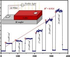
Self-powered visible light photodetector based nanostructured CdSe/Si geometry was fabricated using pulsed laser deposition (PLD). Herein, a detailed microstructural investigation was demonstrated in conjunction with the overall device photoresponsive performance. Particularly, an average particle diameter of 66.62 along optical band gap of 2.25 were attained. This was, subsequently, perceived in the fabricated device spectral response performance during which photocurrent () of 47 µA was attained under incident light of 575 and 6 , the nearest incident wavelength to the obtained optical band gap. At the reported incident light features, the proposed arrangement exhibited responsivity () of 7.85 with light to dark current ratio () of 998 %, respectively. Herein, the incident power variation suggested a linear increment ( 0.94) in both and profiles, with values of 71 µA and 1501 %, respectively, at 575 and 26 . The fabricated device exhibited a pronounced time-resolved feature with rise/fall periods of 0.31 and 0.34 sec., while the power dependance based time-resolved behavior indicated a linear correlation between the stated factors with value of 0.924, both of which were carried out at 0 bias voltage. The dual-singularity evidenced the self-powered feature of the proposed photodetector, where zero external potential is required.
期刊介绍:
Materials Letters has an open access mirror journal Materials Letters: X, sharing the same aims and scope, editorial team, submission system and rigorous peer review.
Materials Letters is dedicated to publishing novel, cutting edge reports of broad interest to the materials community. The journal provides a forum for materials scientists and engineers, physicists, and chemists to rapidly communicate on the most important topics in the field of materials.
Contributions include, but are not limited to, a variety of topics such as:
• Materials - Metals and alloys, amorphous solids, ceramics, composites, polymers, semiconductors
• Applications - Structural, opto-electronic, magnetic, medical, MEMS, sensors, smart
• Characterization - Analytical, microscopy, scanning probes, nanoscopic, optical, electrical, magnetic, acoustic, spectroscopic, diffraction
• Novel Materials - Micro and nanostructures (nanowires, nanotubes, nanoparticles), nanocomposites, thin films, superlattices, quantum dots.
• Processing - Crystal growth, thin film processing, sol-gel processing, mechanical processing, assembly, nanocrystalline processing.
• Properties - Mechanical, magnetic, optical, electrical, ferroelectric, thermal, interfacial, transport, thermodynamic
• Synthesis - Quenching, solid state, solidification, solution synthesis, vapor deposition, high pressure, explosive


 分享
分享
 求助内容:
求助内容: 应助结果提醒方式:
 扫码关注我们
