{"title":"用于有机光电晶体管阵列的高拉伸和定向晶圆级半导体薄膜。","authors":"Xiangxiang Li, Ayesha Sabir, Xiaoying Zhang, Hongchen Jiang, Weiyu Wang, Xinran Zheng and Hui Yang*, ","doi":"10.1021/acsami.4c04349","DOIUrl":null,"url":null,"abstract":"<p >Stretchable organic phototransistor arrays have potential applications in artificial visual systems due to their capacity to perceive ultraweak light across a broad spectrum. Ensuring uniform mechanical and electrical performance of individual devices within these arrays requires semiconductor films with large-area scale, well-defined orientation, and stretchability. However, the progress of stretchable phototransistors is primarily impeded by their limited electrical properties and photodetection capabilities. Herein, wafer-scale and well-oriented semiconductor films were successfully prepared using a solution shearing process. The electrical properties and photodetection capabilities were optimized by improving the polymer chain alignment. Furthermore, a stretchable 10 × 10 transistor array with high device uniformity was fabricated, demonstrating excellent mechanical robustness and photosensitive imaging ability. These arrays based on highly stretchable and well-oriented wafer-scale semiconductor films have great application potential in the field of electronic eye and artificial visual systems.</p>","PeriodicalId":5,"journal":{"name":"ACS Applied Materials & Interfaces","volume":"16 28","pages":"36678–36687"},"PeriodicalIF":8.2000,"publicationDate":"2024-07-05","publicationTypes":"Journal Article","fieldsOfStudy":null,"isOpenAccess":false,"openAccessPdf":"","citationCount":"0","resultStr":"{\"title\":\"Highly Stretchable and Oriented Wafer-Scale Semiconductor Films for Organic Phototransistor Arrays\",\"authors\":\"Xiangxiang Li, Ayesha Sabir, Xiaoying Zhang, Hongchen Jiang, Weiyu Wang, Xinran Zheng and Hui Yang*, \",\"doi\":\"10.1021/acsami.4c04349\",\"DOIUrl\":null,\"url\":null,\"abstract\":\"<p >Stretchable organic phototransistor arrays have potential applications in artificial visual systems due to their capacity to perceive ultraweak light across a broad spectrum. Ensuring uniform mechanical and electrical performance of individual devices within these arrays requires semiconductor films with large-area scale, well-defined orientation, and stretchability. However, the progress of stretchable phototransistors is primarily impeded by their limited electrical properties and photodetection capabilities. Herein, wafer-scale and well-oriented semiconductor films were successfully prepared using a solution shearing process. The electrical properties and photodetection capabilities were optimized by improving the polymer chain alignment. Furthermore, a stretchable 10 × 10 transistor array with high device uniformity was fabricated, demonstrating excellent mechanical robustness and photosensitive imaging ability. These arrays based on highly stretchable and well-oriented wafer-scale semiconductor films have great application potential in the field of electronic eye and artificial visual systems.</p>\",\"PeriodicalId\":5,\"journal\":{\"name\":\"ACS Applied Materials & Interfaces\",\"volume\":\"16 28\",\"pages\":\"36678–36687\"},\"PeriodicalIF\":8.2000,\"publicationDate\":\"2024-07-05\",\"publicationTypes\":\"Journal Article\",\"fieldsOfStudy\":null,\"isOpenAccess\":false,\"openAccessPdf\":\"\",\"citationCount\":\"0\",\"resultStr\":null,\"platform\":\"Semanticscholar\",\"paperid\":null,\"PeriodicalName\":\"ACS Applied Materials & Interfaces\",\"FirstCategoryId\":\"88\",\"ListUrlMain\":\"https://pubs.acs.org/doi/10.1021/acsami.4c04349\",\"RegionNum\":2,\"RegionCategory\":\"材料科学\",\"ArticlePicture\":[],\"TitleCN\":null,\"AbstractTextCN\":null,\"PMCID\":null,\"EPubDate\":\"\",\"PubModel\":\"\",\"JCR\":\"Q1\",\"JCRName\":\"MATERIALS SCIENCE, MULTIDISCIPLINARY\",\"Score\":null,\"Total\":0}","platform":"Semanticscholar","paperid":null,"PeriodicalName":"ACS Applied Materials & Interfaces","FirstCategoryId":"88","ListUrlMain":"https://pubs.acs.org/doi/10.1021/acsami.4c04349","RegionNum":2,"RegionCategory":"材料科学","ArticlePicture":[],"TitleCN":null,"AbstractTextCN":null,"PMCID":null,"EPubDate":"","PubModel":"","JCR":"Q1","JCRName":"MATERIALS SCIENCE, MULTIDISCIPLINARY","Score":null,"Total":0}
Highly Stretchable and Oriented Wafer-Scale Semiconductor Films for Organic Phototransistor Arrays
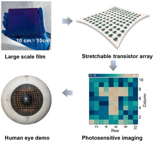
Stretchable organic phototransistor arrays have potential applications in artificial visual systems due to their capacity to perceive ultraweak light across a broad spectrum. Ensuring uniform mechanical and electrical performance of individual devices within these arrays requires semiconductor films with large-area scale, well-defined orientation, and stretchability. However, the progress of stretchable phototransistors is primarily impeded by their limited electrical properties and photodetection capabilities. Herein, wafer-scale and well-oriented semiconductor films were successfully prepared using a solution shearing process. The electrical properties and photodetection capabilities were optimized by improving the polymer chain alignment. Furthermore, a stretchable 10 × 10 transistor array with high device uniformity was fabricated, demonstrating excellent mechanical robustness and photosensitive imaging ability. These arrays based on highly stretchable and well-oriented wafer-scale semiconductor films have great application potential in the field of electronic eye and artificial visual systems.
期刊介绍:
ACS Applied Materials & Interfaces is a leading interdisciplinary journal that brings together chemists, engineers, physicists, and biologists to explore the development and utilization of newly-discovered materials and interfacial processes for specific applications. Our journal has experienced remarkable growth since its establishment in 2009, both in terms of the number of articles published and the impact of the research showcased. We are proud to foster a truly global community, with the majority of published articles originating from outside the United States, reflecting the rapid growth of applied research worldwide.


 分享
分享
 求助内容:
求助内容: 应助结果提醒方式:
 扫码关注我们
