Yu-Seong Seo, Teawoo Ha, Ji Hee Yoo, Su Jae Kim, Yousil Lee, Seungje Kim, Young-Hoon Kim, SeungNam Cha, Young-Min Kim, Se-Young Jeong, Jungseek Hwang
{"title":"单晶铜膜三维多孔纳米结构中的杂散光","authors":"Yu-Seong Seo, Teawoo Ha, Ji Hee Yoo, Su Jae Kim, Yousil Lee, Seungje Kim, Young-Hoon Kim, SeungNam Cha, Young-Min Kim, Se-Young Jeong, Jungseek Hwang","doi":"10.1002/smsc.202400174","DOIUrl":null,"url":null,"abstract":"In the design of optical devices and components, geometric structures and optical properties of materials, such as absorption, refraction, reflection, diffraction, scattering, and trapping, have been utilized. Finding the ideal material with certain optical and geometric characteristics is essential for a customized application. Herein, unoxidizable achromatic copper films (ACFs) are fabricated on Al<sub>2</sub>O<sub>3</sub> substrates utilizing an atomic sputtering epitaxy apparatus. ACFs are made up of two regions vertically: a comparatively flat layer region and a 3D porous nanostructured region on top of the flat region. The measured specular reflectance displays low-pass filter behavior with a sharp cutoff frequency in the infrared spectrum. Furthermore, the measured diffusive reflectance spectra show light-trapping behavior in the spectral region above the cutoff frequency, where there are no known absorption mechanisms, such as phonons and interband transitions. A focused ion beam scanning electron microscope is utilized to study the thin film's nanostructured region through 3D tomographic analysis in order to comprehend the phenomena that are observed. This work will shed fresh light on the design and optimization of optical filters and light-trapping employing porous nanostructured metallic thin films.","PeriodicalId":29791,"journal":{"name":"Small Science","volume":"13 1","pages":""},"PeriodicalIF":8.3000,"publicationDate":"2024-08-02","publicationTypes":"Journal Article","fieldsOfStudy":null,"isOpenAccess":false,"openAccessPdf":"","citationCount":"0","resultStr":"{\"title\":\"Stray Light in 3D Porous Nanostructures of Single-Crystalline Copper Film\",\"authors\":\"Yu-Seong Seo, Teawoo Ha, Ji Hee Yoo, Su Jae Kim, Yousil Lee, Seungje Kim, Young-Hoon Kim, SeungNam Cha, Young-Min Kim, Se-Young Jeong, Jungseek Hwang\",\"doi\":\"10.1002/smsc.202400174\",\"DOIUrl\":null,\"url\":null,\"abstract\":\"In the design of optical devices and components, geometric structures and optical properties of materials, such as absorption, refraction, reflection, diffraction, scattering, and trapping, have been utilized. Finding the ideal material with certain optical and geometric characteristics is essential for a customized application. Herein, unoxidizable achromatic copper films (ACFs) are fabricated on Al<sub>2</sub>O<sub>3</sub> substrates utilizing an atomic sputtering epitaxy apparatus. ACFs are made up of two regions vertically: a comparatively flat layer region and a 3D porous nanostructured region on top of the flat region. The measured specular reflectance displays low-pass filter behavior with a sharp cutoff frequency in the infrared spectrum. Furthermore, the measured diffusive reflectance spectra show light-trapping behavior in the spectral region above the cutoff frequency, where there are no known absorption mechanisms, such as phonons and interband transitions. A focused ion beam scanning electron microscope is utilized to study the thin film's nanostructured region through 3D tomographic analysis in order to comprehend the phenomena that are observed. This work will shed fresh light on the design and optimization of optical filters and light-trapping employing porous nanostructured metallic thin films.\",\"PeriodicalId\":29791,\"journal\":{\"name\":\"Small Science\",\"volume\":\"13 1\",\"pages\":\"\"},\"PeriodicalIF\":8.3000,\"publicationDate\":\"2024-08-02\",\"publicationTypes\":\"Journal Article\",\"fieldsOfStudy\":null,\"isOpenAccess\":false,\"openAccessPdf\":\"\",\"citationCount\":\"0\",\"resultStr\":null,\"platform\":\"Semanticscholar\",\"paperid\":null,\"PeriodicalName\":\"Small Science\",\"FirstCategoryId\":\"1085\",\"ListUrlMain\":\"https://doi.org/10.1002/smsc.202400174\",\"RegionNum\":0,\"RegionCategory\":null,\"ArticlePicture\":[],\"TitleCN\":null,\"AbstractTextCN\":null,\"PMCID\":null,\"EPubDate\":\"\",\"PubModel\":\"\",\"JCR\":\"Q1\",\"JCRName\":\"MATERIALS SCIENCE, MULTIDISCIPLINARY\",\"Score\":null,\"Total\":0}","platform":"Semanticscholar","paperid":null,"PeriodicalName":"Small Science","FirstCategoryId":"1085","ListUrlMain":"https://doi.org/10.1002/smsc.202400174","RegionNum":0,"RegionCategory":null,"ArticlePicture":[],"TitleCN":null,"AbstractTextCN":null,"PMCID":null,"EPubDate":"","PubModel":"","JCR":"Q1","JCRName":"MATERIALS SCIENCE, MULTIDISCIPLINARY","Score":null,"Total":0}
Stray Light in 3D Porous Nanostructures of Single-Crystalline Copper Film
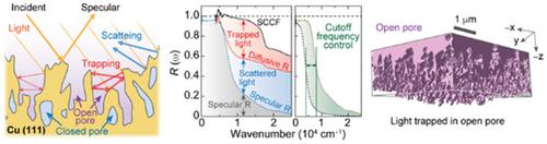
In the design of optical devices and components, geometric structures and optical properties of materials, such as absorption, refraction, reflection, diffraction, scattering, and trapping, have been utilized. Finding the ideal material with certain optical and geometric characteristics is essential for a customized application. Herein, unoxidizable achromatic copper films (ACFs) are fabricated on Al2O3 substrates utilizing an atomic sputtering epitaxy apparatus. ACFs are made up of two regions vertically: a comparatively flat layer region and a 3D porous nanostructured region on top of the flat region. The measured specular reflectance displays low-pass filter behavior with a sharp cutoff frequency in the infrared spectrum. Furthermore, the measured diffusive reflectance spectra show light-trapping behavior in the spectral region above the cutoff frequency, where there are no known absorption mechanisms, such as phonons and interband transitions. A focused ion beam scanning electron microscope is utilized to study the thin film's nanostructured region through 3D tomographic analysis in order to comprehend the phenomena that are observed. This work will shed fresh light on the design and optimization of optical filters and light-trapping employing porous nanostructured metallic thin films.
期刊介绍:
Small Science is a premium multidisciplinary open access journal dedicated to publishing impactful research from all areas of nanoscience and nanotechnology. It features interdisciplinary original research and focused review articles on relevant topics. The journal covers design, characterization, mechanism, technology, and application of micro-/nanoscale structures and systems in various fields including physics, chemistry, materials science, engineering, environmental science, life science, biology, and medicine. It welcomes innovative interdisciplinary research and its readership includes professionals from academia and industry in fields such as chemistry, physics, materials science, biology, engineering, and environmental and analytical science. Small Science is indexed and abstracted in CAS, DOAJ, Clarivate Analytics, ProQuest Central, Publicly Available Content Database, Science Database, SCOPUS, and Web of Science.


 分享
分享
 求助内容:
求助内容: 应助结果提醒方式:
 扫码关注我们
