{"title":"感应峰值带宽增强技术对 CMOS 光放大器噪声性能的影响分析","authors":"Bahram Jalil, Somayeh Kazemi, Mehdi Dolatshahi","doi":"10.1007/s00034-024-02744-9","DOIUrl":null,"url":null,"abstract":"<p>In this paper, the impact of the inductive peaking bandwidth enhancement technique on the input-referred noise performance of a 10 Gbps optical receiver, which includes the CMOS Regulated Cascode (RGC) Transimpedance Amplifier (TIA) is investigated and analyzed. By examining the noise equations in this paper, a novel low-noise design methodology, is introduced. Additionally, through the implementation of the structured <span>\\({\\text{g}}_{\\text{m}}/{\\text{I}}_{\\text{D}}\\)</span> approach and by selecting the suitable transistor dimensions, the power consumption as well as the noise values are reduced, while the values of the obtained gain and bandwidth are increased. To verify the performance of the designed TIA, the circuit is\nsimulated in HSPICE using 90 nm CMOS technology parameters. The simulation results show the obtained gain value of 55.45 dBΩ, a bandwidth of 7.51 GHz and an input referenced noise value of 15.7 pA/√Hz at the 1.2 V power supply, while the circuit consumes 0.75 mW of power.</p>","PeriodicalId":10227,"journal":{"name":"Circuits, Systems and Signal Processing","volume":"81 1","pages":""},"PeriodicalIF":2.0000,"publicationDate":"2024-08-03","publicationTypes":"Journal Article","fieldsOfStudy":null,"isOpenAccess":false,"openAccessPdf":"","citationCount":"0","resultStr":"{\"title\":\"Analysis of the Impact of the Inductive Peaking Bandwidth Enhancement Technique on the Noise Performance of CMOS Optical Amplifiers\",\"authors\":\"Bahram Jalil, Somayeh Kazemi, Mehdi Dolatshahi\",\"doi\":\"10.1007/s00034-024-02744-9\",\"DOIUrl\":null,\"url\":null,\"abstract\":\"<p>In this paper, the impact of the inductive peaking bandwidth enhancement technique on the input-referred noise performance of a 10 Gbps optical receiver, which includes the CMOS Regulated Cascode (RGC) Transimpedance Amplifier (TIA) is investigated and analyzed. By examining the noise equations in this paper, a novel low-noise design methodology, is introduced. Additionally, through the implementation of the structured <span>\\\\({\\\\text{g}}_{\\\\text{m}}/{\\\\text{I}}_{\\\\text{D}}\\\\)</span> approach and by selecting the suitable transistor dimensions, the power consumption as well as the noise values are reduced, while the values of the obtained gain and bandwidth are increased. To verify the performance of the designed TIA, the circuit is\\nsimulated in HSPICE using 90 nm CMOS technology parameters. The simulation results show the obtained gain value of 55.45 dBΩ, a bandwidth of 7.51 GHz and an input referenced noise value of 15.7 pA/√Hz at the 1.2 V power supply, while the circuit consumes 0.75 mW of power.</p>\",\"PeriodicalId\":10227,\"journal\":{\"name\":\"Circuits, Systems and Signal Processing\",\"volume\":\"81 1\",\"pages\":\"\"},\"PeriodicalIF\":2.0000,\"publicationDate\":\"2024-08-03\",\"publicationTypes\":\"Journal Article\",\"fieldsOfStudy\":null,\"isOpenAccess\":false,\"openAccessPdf\":\"\",\"citationCount\":\"0\",\"resultStr\":null,\"platform\":\"Semanticscholar\",\"paperid\":null,\"PeriodicalName\":\"Circuits, Systems and Signal Processing\",\"FirstCategoryId\":\"5\",\"ListUrlMain\":\"https://doi.org/10.1007/s00034-024-02744-9\",\"RegionNum\":3,\"RegionCategory\":\"工程技术\",\"ArticlePicture\":[],\"TitleCN\":null,\"AbstractTextCN\":null,\"PMCID\":null,\"EPubDate\":\"\",\"PubModel\":\"\",\"JCR\":\"Q3\",\"JCRName\":\"ENGINEERING, ELECTRICAL & ELECTRONIC\",\"Score\":null,\"Total\":0}","platform":"Semanticscholar","paperid":null,"PeriodicalName":"Circuits, Systems and Signal Processing","FirstCategoryId":"5","ListUrlMain":"https://doi.org/10.1007/s00034-024-02744-9","RegionNum":3,"RegionCategory":"工程技术","ArticlePicture":[],"TitleCN":null,"AbstractTextCN":null,"PMCID":null,"EPubDate":"","PubModel":"","JCR":"Q3","JCRName":"ENGINEERING, ELECTRICAL & ELECTRONIC","Score":null,"Total":0}
Analysis of the Impact of the Inductive Peaking Bandwidth Enhancement Technique on the Noise Performance of CMOS Optical Amplifiers
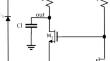
In this paper, the impact of the inductive peaking bandwidth enhancement technique on the input-referred noise performance of a 10 Gbps optical receiver, which includes the CMOS Regulated Cascode (RGC) Transimpedance Amplifier (TIA) is investigated and analyzed. By examining the noise equations in this paper, a novel low-noise design methodology, is introduced. Additionally, through the implementation of the structured \({\text{g}}_{\text{m}}/{\text{I}}_{\text{D}}\) approach and by selecting the suitable transistor dimensions, the power consumption as well as the noise values are reduced, while the values of the obtained gain and bandwidth are increased. To verify the performance of the designed TIA, the circuit is
simulated in HSPICE using 90 nm CMOS technology parameters. The simulation results show the obtained gain value of 55.45 dBΩ, a bandwidth of 7.51 GHz and an input referenced noise value of 15.7 pA/√Hz at the 1.2 V power supply, while the circuit consumes 0.75 mW of power.
期刊介绍:
Rapid developments in the analog and digital processing of signals for communication, control, and computer systems have made the theory of electrical circuits and signal processing a burgeoning area of research and design. The aim of Circuits, Systems, and Signal Processing (CSSP) is to help meet the needs of outlets for significant research papers and state-of-the-art review articles in the area.
The scope of the journal is broad, ranging from mathematical foundations to practical engineering design. It encompasses, but is not limited to, such topics as linear and nonlinear networks, distributed circuits and systems, multi-dimensional signals and systems, analog filters and signal processing, digital filters and signal processing, statistical signal processing, multimedia, computer aided design, graph theory, neural systems, communication circuits and systems, and VLSI signal processing.
The Editorial Board is international, and papers are welcome from throughout the world. The journal is devoted primarily to research papers, but survey, expository, and tutorial papers are also published.
Circuits, Systems, and Signal Processing (CSSP) is published twelve times annually.


 分享
分享
 求助内容:
求助内容: 应助结果提醒方式:
 扫码关注我们
